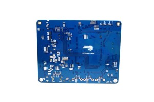
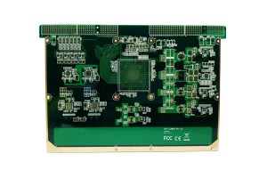
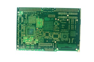
6 Layer ENIG FR4 Blind Vias PCB
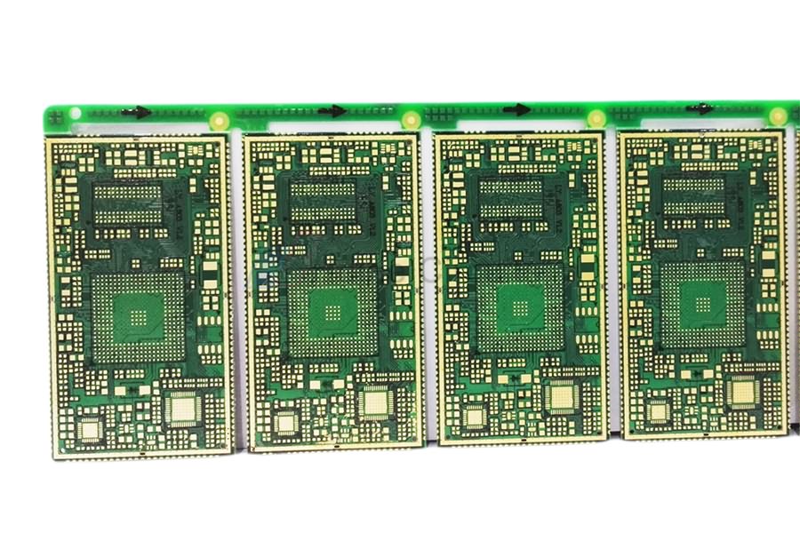
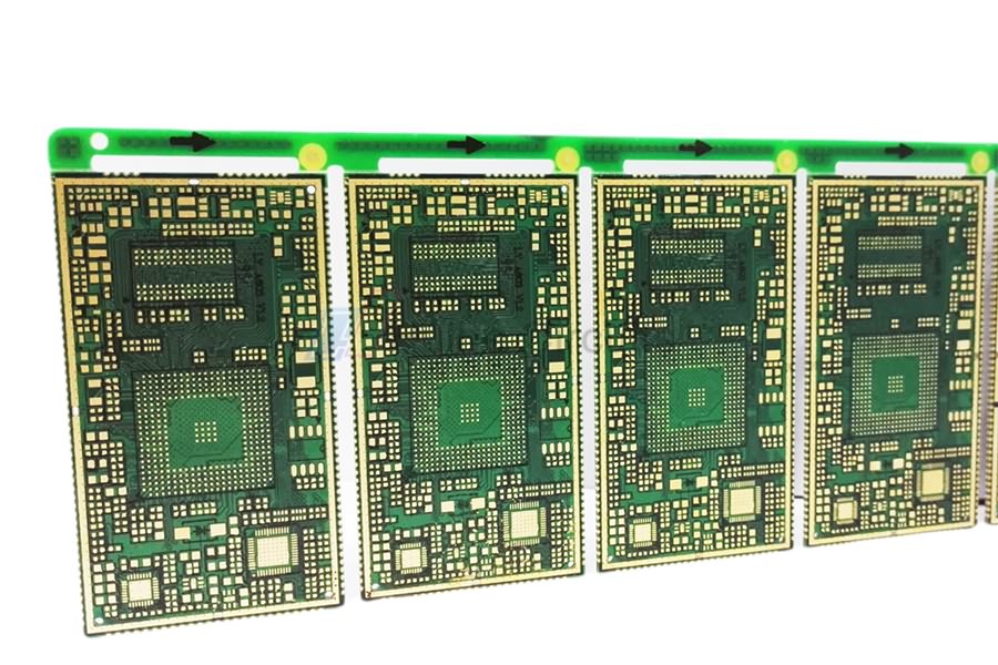
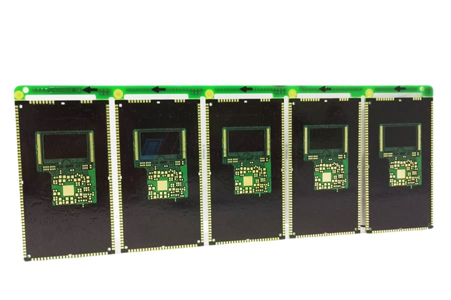
Features Of The Blind Via PCB
Blind Vias are located on the top and bottom surfaces of the circuit board and have a certain depth for the connection between the surface circuit and the inner circuit below. The depth of the hole usually does not exceed a certain ratio (aperture). This way of production will need to pay special attention to the depth of the hole (the Z axis) to the right, do not pay attention to words will cause difficult hole plating so almost no factory used, can also be connected in advance to the layer in the individual circuit when the circuit was first drill hole, and then sticking up, need more precision positioning and contrapuntal device.
Advantage Of The Blind Buried Via PCB
The advantage of blind buried vias PCB for engineers is that the density of components is increased, while the number of layers and size of circuit board are not increased. For electronic products with narrow space and small design tolerance, blind hole design is a good choice. The use of this kind of hole is helpful for circuit design engineers to design reasonable hole/pad ratio and avoid excessive ratio.
Equipment Display

PCB Automatic Plating Line

PCB PTH Line

PCB LDI

PCB CCD Exposure Machine
Factory Show

PCB Manufacturing Base

Admin Receptionist

Meeting Room