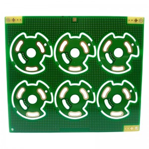
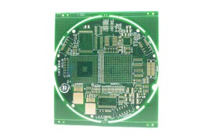
6 Layer HASL Blind Buried Via PCB


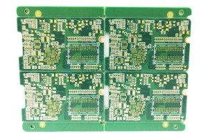
Features Of The Buried Via PCB
The manufacturing process cannot be achieved by drilling after bonding. Drilling must be performed at individual circuit layers. The inner layer must be partially bonded first, followed by electroplating treatment, and then all bonded finally. This process is usually used only on high-density PCBs to increase the available space for other circuit layers
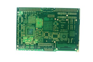
The Basic Process Of HDI Blind Buried Via PCB
Equipment Display

PCB Automatic Plating Line

PCB PTH Line

PCB LDI

PCB CCD Exposure Machine
Write your message here and send it to us