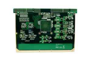
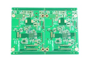
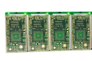
10 Layer ENIG FR4 Blind Vias PCB
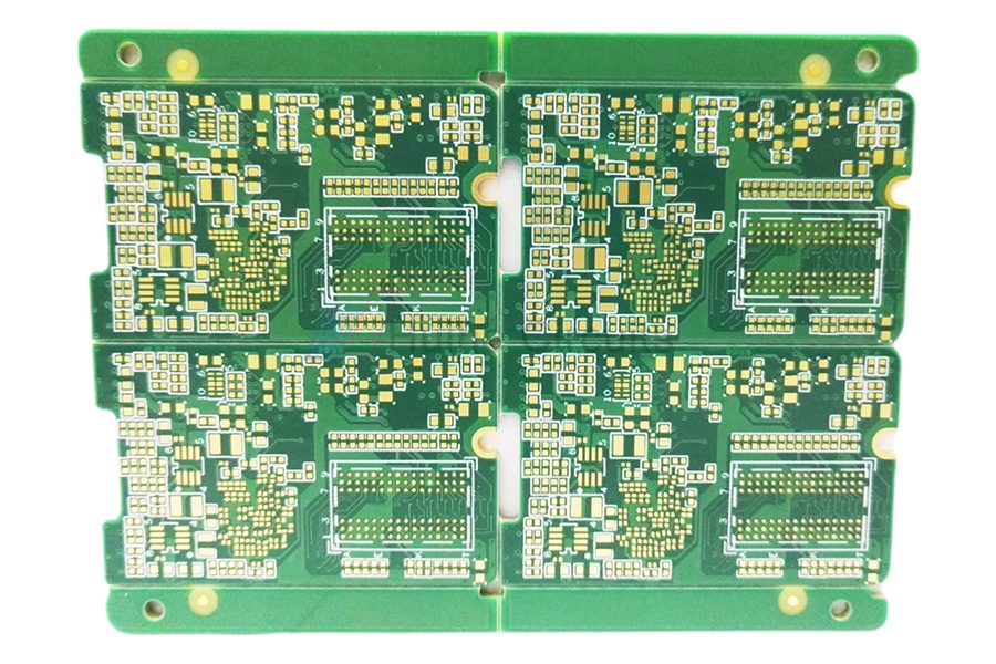

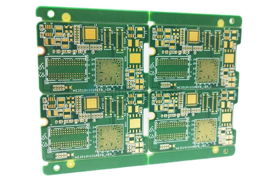
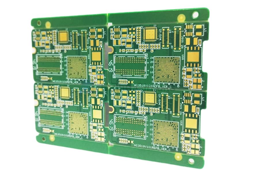
About Blind Buried Via PCB
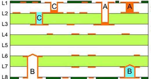
Blind Via: which enables the connection and conduction between the inner and outer layers
Buried Via: which can connect and guide between inner layers Blind Vias are mostly small holes with a diameter of 0.05mm~0.15mm. There are laser hole forming, plasma etched hole and photoinduced hole forming, and laser hole forming is usually used.
HDI: High-density interconnection, non-mechanical drilling, micro-blind hole ring below 6mil, inside and outside layers of wiring line width/line gap is below 4mil, the diameter of the pad is not greater than 0.35mm is called HDI board production mode.
Blind Vias
Blind Vias are used to connect one outer layer to at least one inner layer. Each layer of blind hole needs to generate a separate drill file. The ratio of hole depth to aperture (aspect ratio/thickness-diameter ratio) must be less than or equal to 1. The keyhole determines the hole depth, that is, the maximum distance between the outermost layer and the inner layer.
Equipment Display

PCB Automatic Plating Line

PCB PTH Line

PCB LDI

PCB CCD Exposure Machine
Factory Show

PCB Manufacturing Base

Admin Receptionist

Meeting Room