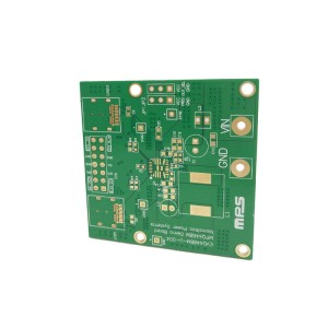
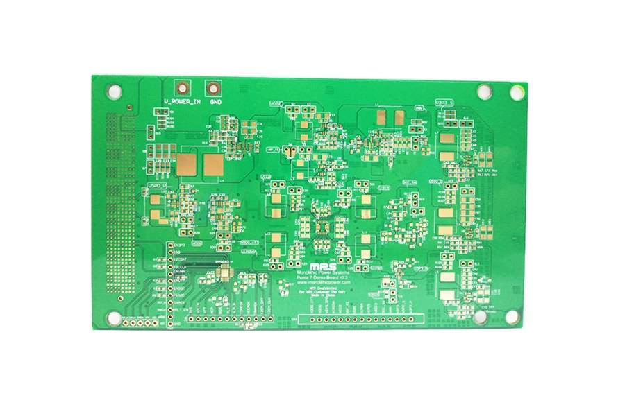
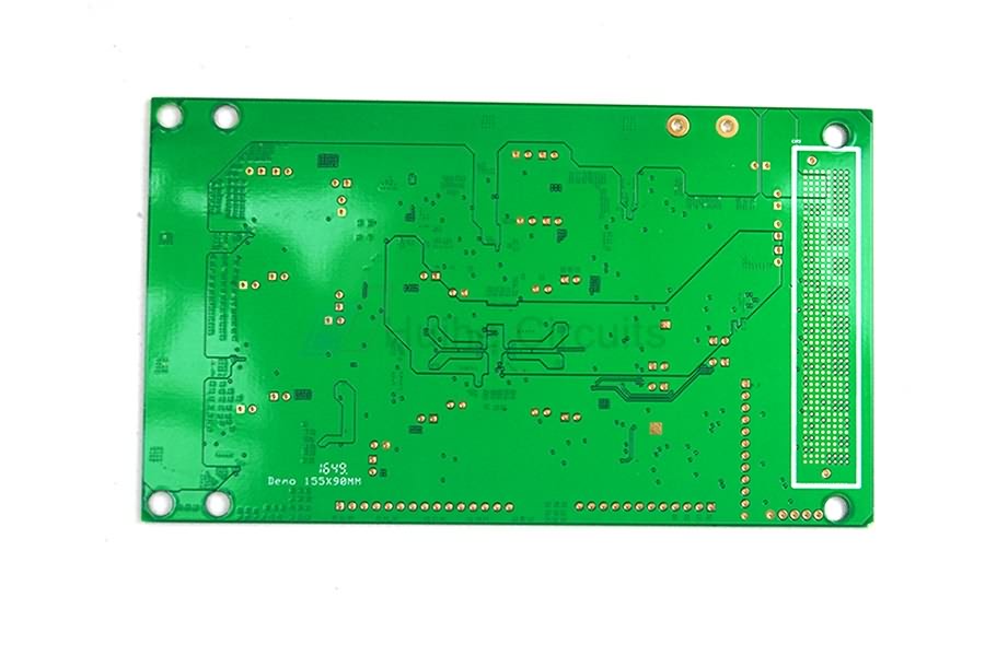
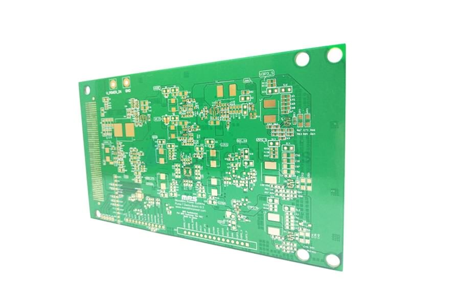
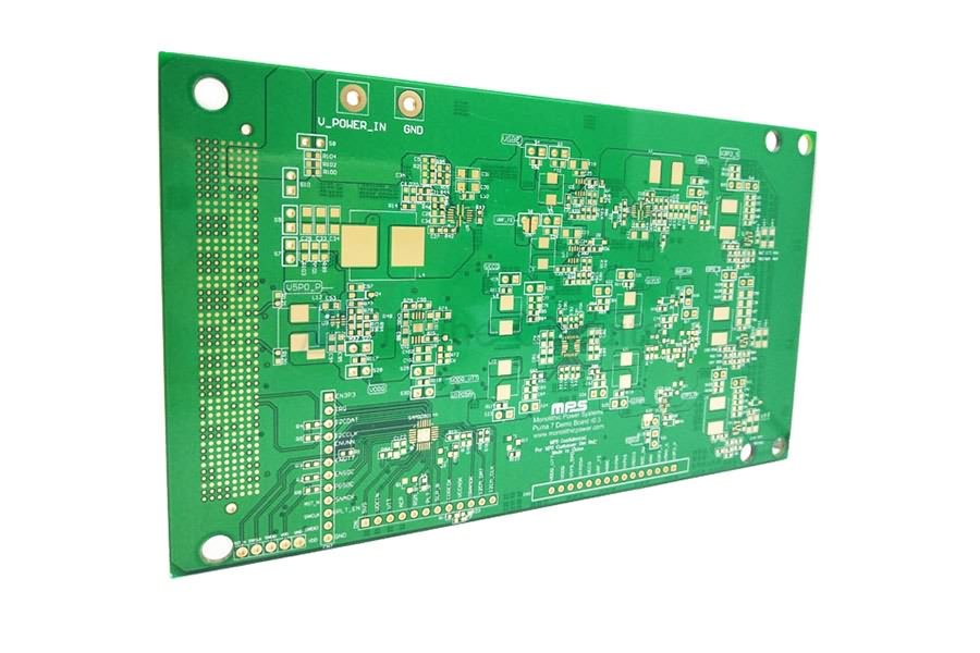
6 Layer ENIG FR4 Heavy Copper PCB
Heavy copper PCB is a layer of copper foil bonded on glass epoxy substrate of printed circuit board. When the thickness of finished copper is more than or equal to 2oz, it is defined as heavy copper PCB. heavy copper PCB has the best extensibility and is not limited by processing temperature. Even in extremely corrosive atmosphere, copper PCB will form a strong and non-toxic passivation protection layer. heavy copper PCB is widely used in various home appliances, high-tech products, military, medical and other electronic equipment. The application of heavy copper PCB makes the circuit board, the core component of electronic equipment products, have longer service life. At the same time, it is helpful to simplify the volume of electronic equipment.
Our Advantage
The highest copper thickness of the sample is 8oz, and the copper thickness is 6oz in mass production
Introduce high precision equipment of PCB industry year by year to ensure excellent PCB process capability
Implement lean production, effectively monitor the production progress and improve the delivery rate
Difficulties In Manufacturing Heavy Copper PCB
1. In the process of etching, if the etching is not clean, the pressure will not reach the standard, which will lead to short circuit of the circuit.
2. Thick copper PCB is easy to foaming agent in the process of solder mask ink manufacturing.
3. The scrap rate of thick copper PCB is the highest in the drilling process, the hole thickness and the nail head are the highest.
4. In the process of pressing, it is easy to appear problems such as insufficient glue filling, too much flowing glue, uneven thickness and voids.