-
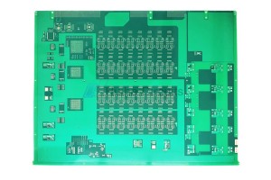
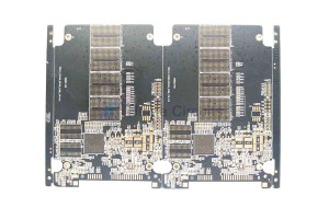
16 Layer ENIG Press Fit Hole PCB
Layers: 16
Surface finish: ENIG
Base material: FR4
Thickness: 3.0mm
Min. hole diameter:0.35mm
Size:420×560mm
Outer Layer W/S: 4/3mil
Inner layer W/S: 5/4mil
Aspect Ratio: 9:1
Special process: via-in-pad, impedance control, press fit hole
-
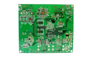
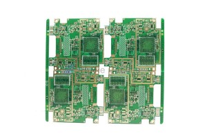
6 Layer ENIG FR4 Via-In-Pad PCB
Layers: 6
Surface finish: ENIG
Base material: FR4
Outer Layer W/S: 4/3.5mil
Inner layer W/S: 4/3.5mil
Thickness: 2.0mm
Min. hole diameter:0.25mm
Special process: via-in-pad, impedance control
-

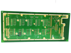
6 Layer ENIG FR4 Via-In-Pad PCB
Layers: 6
Surface finish: ENIG
Base material: FR4
W/S: 5/4mil
Thickness: 1.0mm
Min. hole diameter:0.2mm
Special process: via-in-pad
-
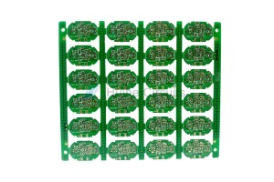
6 Layer ENIG Via-In-Pad PCB
Layers: 6
Surface finish: ENIG
Base material: FR4
Outer Layer W/S: 7/3.5mil
Inner layer W/S: 7/4mil
Thickness: 0.8mm
Min. hole diameter:0.2mm
Special process: via-in-pad
-
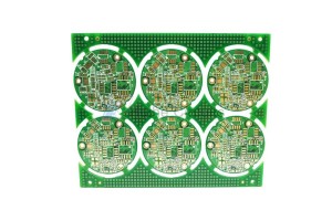
8 Layer ENIG FR4 Via-In-Pad PCB
Layers: 8
Surface finish: ENIG
Base material: FR4
Outer Layer W/S: 4.5/3.5mil
Inner layer W/S: 4.5/3.5mil
Thickness: 1.2mm
Min. hole diameter:0.15mm
Special process: via-in-pad
-
6 Layer FR4 ENIG Via In Pad PCB
Layers: 6
Surface finish: ENIG
Base material: FR4
Outer Layer W/S: 4/3.5mil
Inner layer W/S: 4.5/3.5mil
Thickness: 1.0mm
Min. hole diameter:0.2mm
Special process: via in pad
-
8 Layer ENIG FR4 Via-In-Pad PCB
Layers: 8
Surface finish: ENIG
Base material: FR4
Outer Layer W/S: 4/3.5mil
Inner layer W/S: 4/3.5mil
Thickness: 1.0mm
Min. hole diameter:0.2mm
Special process: via-in-pad, impedance control
-
10 Layer ENIG FR4 Via In Pad PCB
Layer: 10
Surface finish: ENIG
Material: FR4 Tg170
Outer line W/S: 10/7.5mil
Inner line W/S: 3.5/7mil
Board thickness: 2.0mm
Min. hole diameter: 0.15mm
Plug hole: via filling plating


