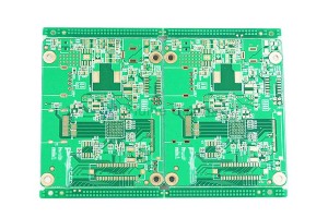
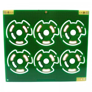
8 Layer ENIG Blind Buried Via PCB
About Level 1 HDI PCB
Level 1 HDI PCB technology refers to the laser blind hole only connected to the surface layer and its adjacent secondary layer hole forming technology.
pressing in one time after drilling →utside again pressing copper foil → and then laser drilling

About Level 1 HDI PCB
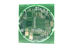
Level 2 HDI PCB
The Level 2 HDI PCB technology is an improvement on the Level 1 HDI PCB technology. It includes two forms of laser blind via drilling directly from the surface layer to the third layer, and laser blind hole drilling directly from the surface layer to the second layer and then from the second layer to the third layer. The difficulty of the Level 2 HDI PCB technology is far greater than the Level 1 HDI PCB technology.
Press in one time after drilling →outside again pressing copper foil →laser, drilling→outer again pressing copper foil→ laser drilling
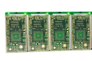
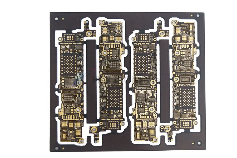
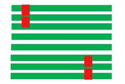
8 layers Of Double Via Level 1 HDI PCB
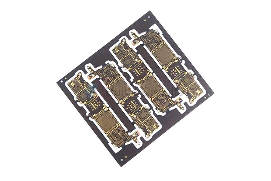
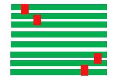
The figure below is 8 layers of level 2 cross blind vias , this processing methodand the above eight layers of second order stack hole , also need to play twolaser perforations . But the perforations are not stacked on top of each othermaking it much less difficult to process.
8 Layers Of Level 2 Cross Blind Vias PCB