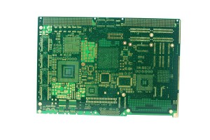
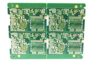
4 Layer ENIG FR4 Blind Buried Vias PCB
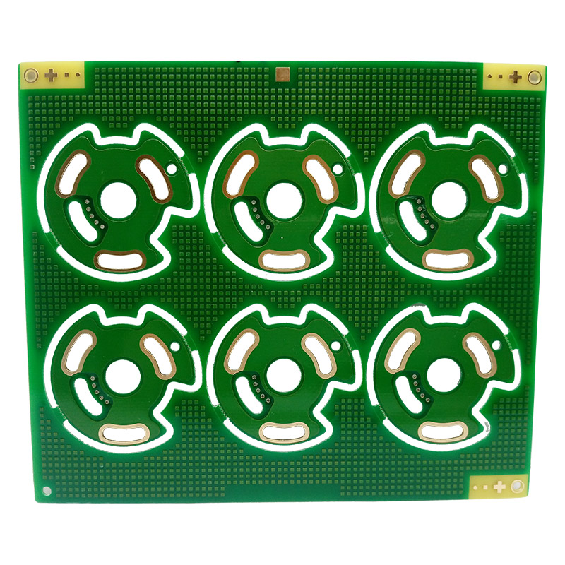
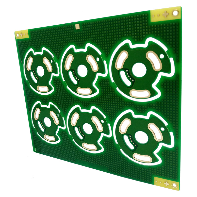
Blind Buried Vias PCB
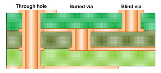
PCB through vias can be divided into through via, blind via and buried via. Blind burrow PCBs may be a solution when you want to place enough PTH vias on the board but space is limited. Blind burrows are used to connect PCB layers within surface limitations. A blind via is an electroplated via that connects only one outer layer to one or more inner layers. Buried vias are electroplated vias that connect two or more inner layers but are not connected to the outer layer.
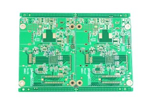
Benefits Of Blind Buried Vias PCB
1. The density limits of wires and pads in the design can be met without increasing the number of layers or circuit board size
2. Reduce the aspect ratio of PCB circuit
Blind via/buried via PCB to meet board density enhancement without increasing the number of layers or board size. Therefore, blind/buried vias are commonly used in HDI PCBs. Often used in mobile phones, wireless communications, MID. The notebook.