-
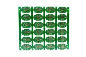
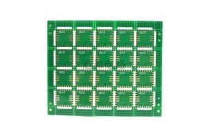
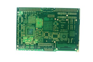
China Wholesale Pcb Order Factories - 6 Layer ENIG via-in-pad PCB 16842 – Huihe
The advantages and disadvantages of plugging and no plugging? In terms of plug holes, they have the following advantages 1. the plug hole can prevent PCB through the wave soldering tin from the through hole through the component surface caused by short circuit; That is to say, within the scope of the wave soldering design area (generally the welding surface is 5mm or above) there is no hole or hole to do plug hole treatment. 2. The plug hole protects against possible short circuits caused by ... -
China Wholesale Single Circuit Board Factories - 8 Layer ENIG Impedance Control PCB 16978 – Huihe
Deficiencies of the blind buried vias The main problem of blind buried via is the high cost. In contrast, buried holes cost less than blind holes, but the use of both types of holes can significantly increase the cost of a board. The cost increase is due to the more complex manufacturing process of the blind buried hole, that is, the increase in manufacturing processes also leads to the increase in testing and inspection processes. Buried Via Buried vias are used to connect differen... -
China Wholesale Redboard Pcb Quotes - 4 Layer ENIG PCB 8329 – Huihe
Manufacturing technology of metallized half hole PCB The metallized half hole is cut in half after the round hole is formed. It is easy to appear the phenomenon of copper wire residue and copper leather warping in the half hole, which affects the function of the half hole and leads to the decrease of product performance and yield. In order to overcome the above defects, it shall be carried out according to the following process steps of metallized semi-orifice PCB 1. Processing half hole... -
China Wholesale Flexible Pcb Fabrication Quotes - 6 layer ENIG impedance control PCB – Huihe
How to improve the lamination quality of multilayer PCB? PCB has developed from single side to double side and multilayer, and the proportion of multilayer PCB is increasing year by year. The performance of multilayer PCB is developing to high precision, dense and fine. Lamination is an important process in multilayer PCB manufacturing. The control of lamination quality is becoming more and more important. Therefore, in order to ensure the quality of multilayer laminate, we need to have ... -
China Wholesale Mp5 Circuit Board Suppliers - 4 Layer ENIG half hole PCB – Huihe
Difficulties in machining metallized half-hole PCB Metalized half-hole PCB after forming the hole wall copper black , burr residuadeviation has been a difficult problem in the molding process of PCB factoEspecially the whole row of half holes similar to stamp holes , the aperture isabout 0.6 mm , the hole wall spacing is 0 . 45 mm , the outer figure spacing is 2mm , because the spacing is very small , it is easy to cause short circuitbecause of copper skin. The general metallized half-ho... -
China Wholesale Silkscreen Circuit Board Suppliers - 8 Layer ENIG Impedance Control PCB 16978 – Huihe
Deficiencies of the blind buried vias The main problem of blind buried via is the high cost. In contrast, buried holes cost less than blind holes, but the use of both types of holes can significantly increase the cost of a board. The cost increase is due to the more complex manufacturing process of the blind buried hole, that is, the increase in manufacturing processes also leads to the increase in testing and inspection processes. Buried Via Buried vias are used to connect differen... -

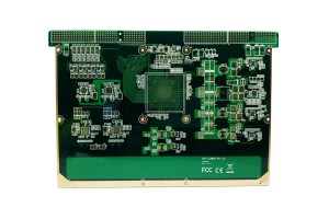
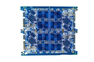
China Wholesale Tht Pcb Factories - 8 Layer ENIG Blind Buried Via PCB 12 – Huihe
About Level 1 Level 1 HDI technology refers to the laser blind hole only connected to the surface layer and its adjacent secondary layer hole forming technology. pressing in one time after drilling →utside again pressing copper foil → and then laser drilling About Level 1 Level 2 HDI PCB The Level 2 HDI technology is an improvement on the Level 1 HDI technology. It includes two forms of laser blind via drilling directly from the surface layer to the third layer, and laser blind... -
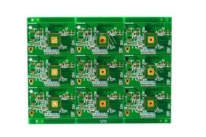
China Wholesale Panel Circuit Board Quotes - 6-layer ENIG impedance control PCB 15749 – Huihe
Differences between multilayer PCB and single panel / double-sided PC The biggest difference between multilayer PCB and single panel and double panel is that the internal power supply layer (to maintain the internal power layer) and the ground layer are added. The power supply and ground wire network are mainly wired on the power supply layer. However, the multilayer wiring is mainly the top and bottom layer, with the middle wiring layer as a supplement. Therefore, the design method of m... -
China Wholesale Automatic Stabilizer Circuit Board Pricelist - 4 Layer OSP Impedance Control PCB 8742 – Huihe
Characteristic impedance control of PCB The characteristic impedance of the conductor on thePCB is an important index of circuit design, especially in the PCB design of high frequency circuit, we must consider whether the characteristic impedance of the conductor is consistent with the characteristic impedance required by the device or signal. PCB impedance matching In the PCB, if there is a signal transmission, it is expected to be from the sending end of the power supply, in the c... -
China Wholesale Universal Pcb Board Manufacturers - 8 Layer ENIG Impedance Control PCB 16978 – Huihe
Deficiencies of the blind buried vias The main problem of blind buried via is the high cost. In contrast, buried holes cost less than blind holes, but the use of both types of holes can significantly increase the cost of a board. The cost increase is due to the more complex manufacturing process of the blind buried hole, that is, the increase in manufacturing processes also leads to the increase in testing and inspection processes. Buried Via Buried vias are used to connect differen... -
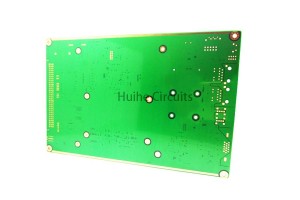
China Wholesale Non Printed Circuit Board Quotes - 8-layer ENIG impedance control PCB 15493 – Huihe
Multilayer PCB design has the following advantages 1.Compared with single-sided PCB and double-sided PCB, it has higher density. 2.No interconnect cable is required. It is the best choice for low weight PCB. 3.Multilayer PCBs have smaller sizes and save space. 4.EMI is very simple and flexible. 5.Durable and powerful. Application of multilayer PCB Multilayer PCB design is the basic requirement of many electronic components: accelerator Mobile transmission Optical fiber Scanning tech... -
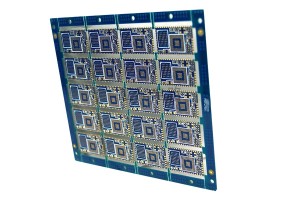
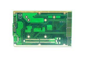
China Wholesale Pcb Printing Manufacturers - 14 Layer Blind Buried Via PCB – Huihe
About Blind Buried Via PCB Blind vias and buried vias are two ways to establish connections between layers of printed circuit board. The blind vias of the printed circuit board are copper-plated vias that can be connected to the outer layer through most of the inner layer. The burrow connects two or more inner layers but does not penetrate the outer layer. Use microblind vias to increase line distribution density, improve radio frequency and electromagnetic interference, heat conduction,...


