-

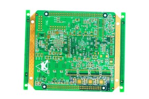
China Wholesale Smt Boards Quotes - 6 layer ENIG Impedance Control Heavy Copper PCB 15881 – Huihe
Functions of heavy copper PCB Heavy copper PCB has the best extension functions, is not limited by the processing temperature, high melting point can be used oxygen blowing, low temperature at the same brittle and other hot melt welding, but also fire prevention, belongs to the non-combustible material. Even in highly corrosive atmospheric conditions, copper sheets form a strong, non-toxic passivation protective layer. Difficulty in machining control of heavy copper PCB Thickness of copper PC... -

China Wholesale Universal Pcb Board Pricelist - 8 layer ENIG Impedance Control Heavy Copper PCB 16555 – Huihe
Thin core heavy copper PCB copper foil choice The most concerned problem of heavy copper CCL PCB is the pressure resistance problem, especially the thin core heavy copper PCB (thin core is medium thickness ≤ 0.3mm), the pressure resistance problem is particularly prominent, thin core heavy copper PCB will generally choose RTF copper foil for production, RTF copper foil and STD copper foil main difference is the length of the wool Ra is different, RTF copper foil Ra is significantly less ... -
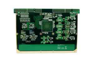
China Wholesale Emc Pcb Quotes - 16 Layer High TG ENIG PCB – Huihe
High Tg PCB circuit board is basically defined as PCB raw material or designed to withstand high heat resistance in high temperature PCB, high Tg is usually higher than 170 ° C. Therefore, the PCB with TG greater than or equal to 170 ° C is high Tg PCB, which can also be called glass transition temperature. High heat resistance, commonly used in lead-free process. Our advantage 1. Own factory, factory area 12000 square meters, factory direct sales 2. Product 100% test (AOI scanning, 100%... -
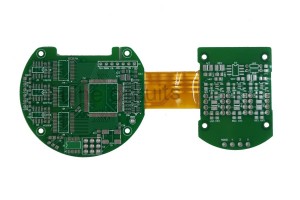
China Wholesale Pcb Order Manufacturers - 4 Layer SF302+FR4 Rigid-Flex PCB 19 – Huihe
Points for attention in the design of rigid flexible combination zone 1.The line should transition smoothly, and the direction of the line should be perpendicular to the bending direction. 2.The conductor shall be evenly distributed throughout the bending zone. 3.The width of the conductor shall be maximized throughout the bending zone. 4.PTH design should not be used in rigid flexible transition zone. 5.Bending radius of bending zone of rigid flexible PCB Material of flexible PCB E... -
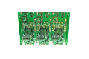
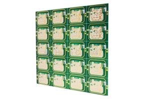
China Wholesale Pcb Stripboard Manufacturers - 6 Layer ENIG Blind Vias PCB 27809 – Huihe
Features of the Blind Via Blind Vias are located on the top and bottom surfaces of the circuit board and have a certain depth for the connection between the surface circuit and the inner circuit below. The depth of the hole usually does not exceed a certain ratio (aperture). This way of production will need to pay special attention to the depth of the hole (the Z axis) to the right, do not pay attention to words will cause difficult hole plating so almost no factory used, can also be connecte... -
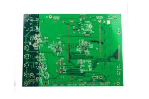
China Wholesale Smt Boards Manufacturers - 6 Layer ENIG Impedance Control PCB 7201 – Huihe
PCB impedance line design 1.In the process of PCB LAYOUT, consider the basic conditions required to control the impedance are: line width, line distance, line length, impedance line shielding reference layer, according to these requirements will be placed in the appropriate position of the impedance line. 2. The shielding reference layer preferentially selects the line adjacent to the layer where the impedance line is located. The corresponding position of the impedance line is a complete cop... -
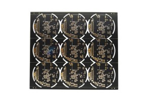
China Wholesale Pcb Clad Board Quotes - 8 Layer ENIG Impedance Control PCB 16978 – Huihe
Deficiencies of the blind buried vias The main problem of blind buried via is the high cost. In contrast, buried holes cost less than blind holes, but the use of both types of holes can significantly increase the cost of a board. The cost increase is due to the more complex manufacturing process of the blind buried hole, that is, the increase in manufacturing processes also leads to the increase in testing and inspection processes. Buried Via Buried vias are used to connect differen... -
China Wholesale Solder Circuit Board Suppliers - 4 Layer ENIG Impedance Control PCB 9115 – Huihe
About the impedance control In the case of transmission of high frequency signals, the controlled impedance helps to ensure that the signal does not decay significantly during transmission. In essence, controlled impedance refers to the matching of the material properties of the substrate to the characteristics of the line/dielectric layer to ensure that the impedance value of the line signal is within the tolerance of the reference value. Controlled impedance PCBs provide reliable and c... -
China Wholesale Eft Printed Circuit Board Pricelist - 6 layer ENIG Heavy Copper PCB 15202 – Huihe
Crack problem of inner thick brazing pad The demand for heavy copper PCB is increasing, and the inner layer pads are getting smaller and smaller. The problem of pad cracking often occurs during PCB drilling (mainly for large holes above 2.5mm). There is little room for improvement in the material aspect of this kind of problem. The traditional improvement method is to increase the pad, increase the peeling strength of the material, and reduce the drilling rate, etc. Based on the analysis... -
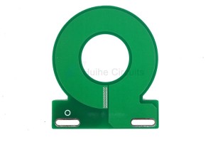
China Wholesale Circular Circuit Board Quotes - 2 Layer High TG Heavy Copper PCB 11 – Huihe
About the heavy copper PCB Heavy copper PCB has the characteristics of carrying large current, reducing thermal strain and good heat dissipation. Increasing copper thickness has become an effective way for many terminal design manufacturers to seek solutions. There are more and more heavy copper PCB products, as a special product in product design, CCL production and PCB processing, there are many production difficulties and matters needing attention and solution. CCL is the raw material... -
China Wholesale Prototype Pcb Assembly Quotes - 4 Layer Rogers ENIG PCB 25770 – Huihe
Transmission line form in high frequency PCB design Both transmission lines and waveguides can be used as carriers for high frequency signal transmission, while microstrip lines and strip lines in TEM transmission lines and Substrate Integrated Waveguide in Waveguide structures are applied in the design of high frequency PCBs. High frequency PCB wiring skills The radiation intensity of the signal is proportional to the wiring length of the signal line. The longer the high-frequency ... -
China Wholesale Circuit Board Makers Manufacturers - 4 Layer Rogers ENIG PCB 25770 – Huihe
Transmission line form in high frequency PCB design Both transmission lines and waveguides can be used as carriers for high frequency signal transmission, while microstrip lines and strip lines in TEM transmission lines and Substrate Integrated Waveguide in Waveguide structures are applied in the design of high frequency PCBs. High frequency PCB wiring skills The radiation intensity of the signal is proportional to the wiring length of the signal line. The longer the high-frequency ...


