-
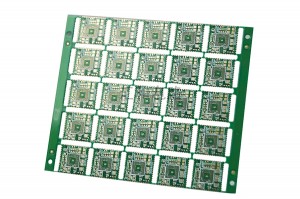
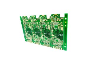
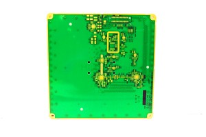
China Wholesale Motherboard Circuit Board Manufacturers - 4 Layer ENIG half hole PCB 12026 – Huihe
Difficulties in machining metallized half-hole PCB Metalized half-hole PCB after forming the hole wall copper black, burr residual, deviation has been a difficult problem in the molding process of PCB factory. Especially the whole row of half holes similar to stamp holes, the aperture is about 0.6 mm, the hole wall spacing is 0.45 mm, the outer figure spacing is 2 mm, because the spacing is very small, it is easy to cause short circuit because of copper skin. The general metallized half-hole ... -
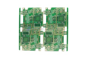
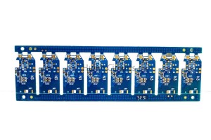
China Wholesale Rigid Flex Circuit Boards Manufacturers - 8 Layer ENIG via-in-pad PCB 16081 – Huihe
Resin plugging process 1. Definition Resin plugging process refers to the use of resin to plug the buried holes in the inner layer, and then press, which is widely used in high-frequency board and HDI board; it is divided into traditional screen printing Resin Plugging and vacuum resin plugging. Generally, the production process of the product is traditional screen printing resin plug hole, which is also the most common process in the industry. 2. Process Pre process — drilling resin hole — e... -
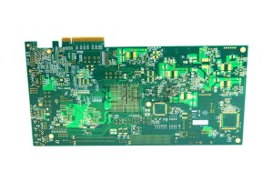
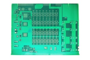
China Wholesale Mosfet Pcb Quotes - 10 Layer Medium TG Gold Finger PCB – Huihe
The advantages of high Tg materials The main advantage of high Tg materials is higher operating temperature( MOT ) , which can carry more current . According to experience , TG minusabout 20 C can be used as mot . At this temperature , the PCB can runnormally for a long time without damage. The heat resistance temperature of the common solder mask is usually lowerthan the Tg of the substrate . The conventional maximum operatingtemperature of solder mask is about 150 C . For high Tg appli... -
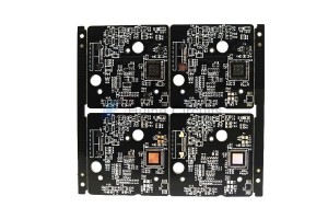
China Wholesale Mini Pcb Board Pricelist - 4 layer HASL Impedance Control Heavy Copper PCB 16116 – Huihe
Advantages and functions of heavy copper PCB Functions: The application of heavy copper PCB in PCB proofing is almost everywhere, and its application field is very broad, including all kinds of home appliances, high-tech products, military, medical and other electronic equipment. Heavy copper PCB has excellent extension performance, high temperature, low temperature, corrosion resistance, so that electronic equipment products have a longer service life, but also to simplify the volume of... -

China Wholesale Bluetooth Pcb Board Manufacturers - 6 Layer Rogers+ FR4 PCB – Huihe
The electrical, thermal and mechanical properties of high-frequency materials are different from those of conventional FR-4 materials. High frequency PCB has low dielectric constant Dk, low transmission delay, low loss factor Df and low dielectric loss. The high-frequency microwave board and RF board produced by Huihe Circuit include 5G base station antenna circuit board, 4G intermodulation antenna circuit board, high-precision impedance circuit board, high-frequency high-speed mixed voltage ... -
China Wholesale Rohs Pcb Quotes - 6 Layer ENIG Impedance Control PCB 14706 – Huihe
Difference between pad and via 1. Definitions differ Pad: is the basic unit of surface mount assembly, which is used to form the landpattern of the circuit board, that is, a variety of combinations of pads designed for special component types. Through hole: through hole is also called metallization hole. In the double panel and multilayer PCB, a common hole is drilled at the junction of the wires that need to be connected between the layers in order to connect the printed wires between l... -
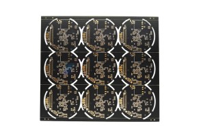
China Wholesale Printed Wiring Board Assembly Quotes - 16 Layer ENIG Press Fit Hole PCB 31525 – Huihe
About Via-In-Pad PCB The Via-In-Pad PCBs are generally blind holes, which are mainly used to connect the inner layer or the secondary outer layer of HDI PCB with the outer layer, so as to improve the electrical performance and reliability of electronic products, shorten the signal transmission wire, reduce the inductive reactance and capacitive reactance of the transmission line, as well as the internal and external electromagnetic interference. It’s used for conducting. The main problem... -
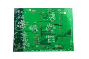
China Wholesale Printed Circuit Board Assembly Pricelist - 6 layer ENIG Heavy Copper PCB 15202 – Huihe
Crack problem of inner thick brazing pad The demand for heavy copper PCB is increasing, and the inner layer pads are getting smaller and smaller. The problem of pad cracking often occurs during PCB drilling (mainly for large holes above 2.5mm). There is little room for improvement in the material aspect of this kind of problem. The traditional improvement method is to increase the pad, increase the peeling strength of the material, and reduce the drilling rate, etc. Based on the analysis... -
China Wholesale Impedance Control In Pcb Factories - 6 Layer ENIG Impedance Control PCB 7201 – Huihe
PCB impedance line design 1.In the process of PCB LAYOUT, consider the basic conditions required to control the impedance are: line width, line distance, line length, impedance line shielding reference layer, according to these requirements will be placed in the appropriate position of the impedance line. 2. The shielding reference layer preferentially selects the line adjacent to the layer where the impedance line is located. The corresponding position of the impedance line is a complete cop... -
China Wholesale Lcd Pcb Board Quotes - 6 Layer ENIG Impedance Control PCB 7201 – Huihe
PCB impedance line design 1.In the process of PCB LAYOUT, consider the basic conditions required to control the impedance are: line width, line distance, line length, impedance line shielding reference layer, according to these requirements will be placed in the appropriate position of the impedance line. 2. The shielding reference layer preferentially selects the line adjacent to the layer where the impedance line is located. The corresponding position of the impedance line is a complete cop... -
China Wholesale Circular Circuit Board Suppliers - 6 Layer FR4+Rogers PCB 28727 – Huihe
Features of high frequency PCB 1. High frequency PCB with small dielectric constant, loss will be very small, and advanced induction heating technology can achieve the needs of the target heating, very high efficiency. Of course, while paying attention to efficiency, it also has the characteristics of environmental protection, which is very suitable for the development direction of today’s society. 2. The transmission speed is inversely proportional to the square root of the dielec... -
China Wholesale Pcb Tg Manufacturers - 8 layer HASL PCB circuit board – Huihe
Why are multilayer boards mostly even? Due to the lack of a layer of medium and foil, the cost of raw materials for odd PCB is slightly lower than that for even PCB. However, the processing cost of odd layer PCB is significantly higher than that of even layer PCB. The processing cost of the inner layer is the same, but the foil/core structure significantly increases the processing cost of the outer layer. Odd layer PCB needs to add non-standard lamination core layer bonding process on th...


