-
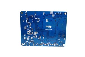
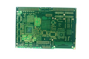
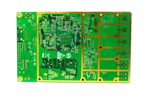
China Wholesale Stabilizer Pcb Board Factories - 6 Layer HASL Blind Buried Via PCB 13699 – Huihe
Features of the Buried Via The manufacturing process cannot be achieved by drilling after bonding. Drilling must be performed at individual circuit layers. The inner layer must be partially bonded first, followed by electroplating treatment, and then all bonded finally. This process is usually used only on high-density PCBs to increase the available space for other circuit layers The basic process of making HDI blind buried Via PCB Equipment display Automatic Plating Lin... -
China Wholesale Motion Sensor Circuit Board Quotes - 4 Layer OSP Impedance Control PCB 8742 – Huihe
Characteristic impedance control of PCB The characteristic impedance of the conductor on thePCB is an important index of circuit design, especially in the PCB design of high frequency circuit, we must consider whether the characteristic impedance of the conductor is consistent with the characteristic impedance required by the device or signal. PCB impedance matching In the PCB, if there is a signal transmission, it is expected to be from the sending end of the power supply, in the c... -
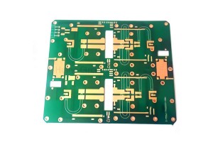
China Wholesale Castellated Pcb Factories - 4 Layer FR4+Rogers PCB 28848 – Huihe
The difficulty of laminated structure of mixed press PCB One of the major challenges in RF/microwave applications is how to ensure that the actual tolerances are within the design tolerances, so as to achieve the desired operating frequency. One of the biggest challenges in the lamination design of mixed-pressure structures is to have uniform thickness between different panels or even between different pieces. Due to the existence of a variety of substrate material types, there are a variety ... -
China Wholesale Pcb Assembly Manufacturers - 6 Layer HASL Blind Buried Via PCB 13699 – Huihe
Features of the Buried Via The manufacturing process cannot be achieved by drilling after bonding. Drilling must be performed at individual circuit layers. The inner layer must be partially bonded first, followed by electroplating treatment, and then all bonded finally. This process is usually used only on high-density PCBs to increase the available space for other circuit layers The basic process of making HDI blind buried Via PCB Equipment display Automatic Plating Lin... -
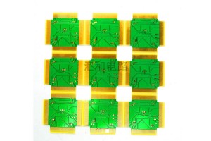
China Wholesale Fast Pcb Prototyping Service Pricelist - 6 Layer FPC+FR4 Rigid-Flex PCB 9 – Huihe
About the Rigid-Flex PCB Rigid-flex PCB is a new type of PCB with both the durability of rigid pcb and the adaptability of flexible PCB. In all types of PCB, the rigid-flex PCB is the most resistant to harsh application environment. Therefore, it is favored by industrial control, medical and military equipment manufacturers. The rigid-flex PCB factories in the mainland are gradually increasing the proportion of flexible and rigid PCB in the total output. Advantages and disadvantages of Rigid-... -
China Wholesale Double Sided Pcb Board Prototype Factories - 14 Layer Blind Buried Via PCB – Huihe
About Blind Buried Via PCB Blind vias and buried vias are two ways to establish connections between layers of printed circuit board. The blind vias of the printed circuit board are copper-plated vias that can be connected to the outer layer through most of the inner layer. The burrow connects two or more inner layers but does not penetrate the outer layer. Use microblind vias to increase line distribution density, improve radio frequency and electromagnetic interference, heat conduction,... -
China Wholesale Pcb Fabrication Service Suppliers - 2 layer High TG ENIG PCB 11590 – Huihe
About High Tg material Tg is the mechanical property that specifies the glass transition temperature, the maximum temperature at which the glass remains rigid.Normal PCB FR4-TG is 130-140 degrees, medium TG is greater than 150-160 degrees, high TG is greater than 170 degrees. Compared with standard FR4, high FR4-TG has better mechanical and chemical heat resistance and moisture resistance.The higher the Tg value, the better the heat resistance of the material, so, especially in the lead-... -
China Wholesale Best Pcb Pricelist - 4 layer Taconic ENIG PCB 53 – Huihe
About PTFE PCB PTFE (commonly known as Teflon) is an ideal dielectric for RF applications, but it is not easily compatible with the conventional dielectric FR4 in PCB manufacturing. Ceramic dielectric is the most commonly used dielectric material in multilayer PCB. It can be used as a separate dielectric layer in special applications and as an inner dielectric layer in FR4 laminated structure in conventional applications. Many RF signal layers of RF design have large non copper filled ar... -

China Wholesale Flex Printed Circuit Suppliers - 6 Layer ENIG Impedance Control PCB 10222 – Huihe
Factors determining controlled impedance The characteristic impedance of a PCB is usually determined by its inductance and capacitance, resistance and conductance. These factors are functions of the physical size of the circuit, the dielectric constant and dielectric thickness of the PCB substrate material. In general, the line impedance of a PCB ranges from 25 to 125Ω. The PCB structure that determines the impedance value consists of the following factors: Width and thickness of top and... -
China Wholesale Pcb Board Supplier Pricelist - 6 layer ENIG impedance control PCB 16403 – Huihe
About Multilayer PCB With the increasing complexity of circuit design, in order to increase the area of wiring, multilayer PCB can be used. Multilayer board is a PCB that contains multiple working layers. In addition to the top and bottom layers, it also includes signal layer, middle layer, internal power supply and ground layer. The number of layers of PCB represents that there are several independent wiring layers. Generally, the number of layers is even and includes the outermost two ... -
China Wholesale Silkscreen Circuit Board Manufacturers - 8 Layer ENIG Impedance Control PCB – Huihe
Impedance is the combination of capacitance and inductance to hinder the circuit under high frequency signal. Impedance is an AC characteristic, which means it is frequency dependent. In the case of transmitting high-frequency signals, the controlled impedance helps to ensure that there is no significant attenuation of the signal during transmission. In essence, the controlled impedance means that the material characteristics of the substrate match the characteristics of the line / dielectric... -
China Wholesale Silkscreen Circuit Board Pricelist - 8 Layer ENIG Impedance Control PCB 16978 – Huihe
Deficiencies of the blind buried vias The main problem of blind buried via is the high cost. In contrast, buried holes cost less than blind holes, but the use of both types of holes can significantly increase the cost of a board. The cost increase is due to the more complex manufacturing process of the blind buried hole, that is, the increase in manufacturing processes also leads to the increase in testing and inspection processes. Buried Via Buried vias are used to connect differen...


