-
China Wholesale Populated Printed Circuit Boards Factories - 10 layer ENIG impedance control PCB – Huihe
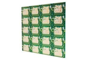
About Multilayer PCB Multilayer PCB refers to the multilayer PCB used in electrical products, multilayer board using more single or double panel wiring board. With a double lining, two one-way for outer layer or two double lining, two blocks of single outer layer of the printed circuit board, through the positioning and alternate insulation adhesive materials and conductive graphics interconnection according to design requirement of printed circuit board becomes four, six layer PCB, also... -
China Wholesale Tht Pcb Quotes - 6 Layer High TG Leadless Golden Finger PCB – Huihe
When need high temperature PCBs? If the working temperature of the product is higher than 130 ℃, a high Tg PCB is required to ensure safety. The main reason for using high Tg PCB is that the PCB needs to comply with RoHS directive, and the temperature required for lead-free solder flow is high, resulting in the substrate of printed circuit board needs to be high Tg material. Application of the High Tg PCB TG PCB is used in electronic industry which can run at higher temperature. By ... -
China Wholesale Hitech Pcb Manufacturers - 4 Layer OSP Impedance Control PCB 8742 – Huihe
Characteristic impedance control of PCB The characteristic impedance of the conductor on thePCB is an important index of circuit design, especially in the PCB design of high frequency circuit, we must consider whether the characteristic impedance of the conductor is consistent with the characteristic impedance required by the device or signal. PCB impedance matching In the PCB, if there is a signal transmission, it is expected to be from the sending end of the power supply, in the c... -
China Wholesale Rohs Pcb Manufacturers - 4 Layer ENIG Blind Buried Via PCB – Huihe
About the HDI Due to the influence of drilling tool, the cost of traditional PCB drilling is very high when the drilling diameter reaches 0.15mm, and it is difficult to improve again. The drilling of HDI board no longer depends on the traditional mechanical drilling, but uses laser drilling technology. (so it is sometimes called laser plate.) The drilling hole diameter of HDI board is generally 3-5mil (0.076-0.127mm), and the line width is generally 3-4mil (0.076-0.10mm). The size of pad... -
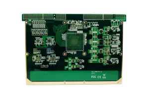
China Wholesale Single Circuit Board Factories - 8 Layer ENIG Impedance Control PCB 16978 – Huihe
Deficiencies of the blind buried vias The main problem of blind buried via is the high cost. In contrast, buried holes cost less than blind holes, but the use of both types of holes can significantly increase the cost of a board. The cost increase is due to the more complex manufacturing process of the blind buried hole, that is, the increase in manufacturing processes also leads to the increase in testing and inspection processes. Buried Via Buried vias are used to connect differen... -
China Wholesale Euro Pcb Suppliers - 4 layer HASL Impedance Control Heavy Copper PCB 16116 – Huihe
Advantages and functions of heavy copper PCB Functions: The application of heavy copper PCB in PCB proofing is almost everywhere, and its application field is very broad, including all kinds of home appliances, high-tech products, military, medical and other electronic equipment. Heavy copper PCB has excellent extension performance, high temperature, low temperature, corrosion resistance, so that electronic equipment products have a longer service life, but also to simplify the volume of... -
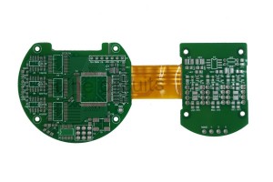
China Wholesale Non Printed Circuit Board Factories - 4 Layer SF302+FR4 Rigid-Flex PCB 19 – Huihe
Points for attention in the design of rigid flexible combination zone 1.The line should transition smoothly, and the direction of the line should be perpendicular to the bending direction. 2.The conductor shall be evenly distributed throughout the bending zone. 3.The width of the conductor shall be maximized throughout the bending zone. 4.PTH design should not be used in rigid flexible transition zone. 5.Bending radius of bending zone of rigid flexible PCB Material of flexible PCB E... -
China Wholesale Printed Wiring Board Assembly Suppliers - 6 layer ENIG impedance control PCB – Huihe
How to improve the lamination quality of multilayer PCB? PCB has developed from single side to double side and multilayer, and the proportion of multilayer PCB is increasing year by year. The performance of multilayer PCB is developing to high precision, dense and fine. Lamination is an important process in multilayer PCB manufacturing. The control of lamination quality is becoming more and more important. Therefore, in order to ensure the quality of multilayer laminate, we need to have ... -
China Wholesale Custom Circuit Board Factories - 4 Layer Rogers ENIG PCB 25770 – Huihe
Transmission line form in high frequency PCB design Both transmission lines and waveguides can be used as carriers for high frequency signal transmission, while microstrip lines and strip lines in TEM transmission lines and Substrate Integrated Waveguide in Waveguide structures are applied in the design of high frequency PCBs. High frequency PCB wiring skills The radiation intensity of the signal is proportional to the wiring length of the signal line. The longer the high-frequency ... -
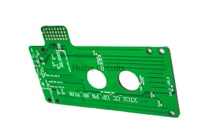
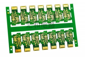
China Wholesale Speaker Circuit Board Quotes - 4 Layer ENIG impedance half hole PCB 13633 – Huihe
Half hole splicing mode By using the stamp hole splicing method, the purpose is to make the connecting bar between the small plate and the small plate. In order to facilitate the cutting, some holes will be opened on the top of the bar (the diameter of the conventional hole is 0.65-0.85 MM), which is the stamp hole. Now the board has to pass the SMD machine, so when you do the PCB, you can connect the board too many PCB. at a time After the SMD, the back board should be separated, and th... -
China Wholesale Circuit Board Assembly Factories - 6-layer ENIG impedance control PCB 15749 – Huihe
Differences between multilayer PCB and single panel / double-sided PC The biggest difference between multilayer PCB and single panel and double panel is that the internal power supply layer (to maintain the internal power layer) and the ground layer are added. The power supply and ground wire network are mainly wired on the power supply layer. However, the multilayer wiring is mainly the top and bottom layer, with the middle wiring layer as a supplement. Therefore, the design method of m... -

China Wholesale Small Pcb Board Pricelist - 6 Layer ENIG Impedance Control PCB 10222 – Huihe
Factors determining controlled impedance The characteristic impedance of a PCB is usually determined by its inductance and capacitance, resistance and conductance. These factors are functions of the physical size of the circuit, the dielectric constant and dielectric thickness of the PCB substrate material. In general, the line impedance of a PCB ranges from 25 to 125Ω. The PCB structure that determines the impedance value consists of the following factors: Width and thickness of top and...


