-
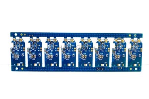
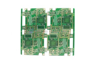
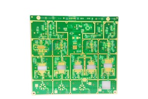
China Wholesale Automatic Stabilizer Circuit Board Pricelist - 8 layer HASL PCB circuit board – Huihe
Why are multilayer boards mostly even? Due to the lack of a layer of medium and foil, the cost of raw materials for odd PCB is slightly lower than that for even PCB. However, the processing cost of odd layer PCB is significantly higher than that of even layer PCB. The processing cost of the inner layer is the same, but the foil/core structure significantly increases the processing cost of the outer layer. Odd layer PCB needs to add non-standard lamination core layer bonding process on th... -
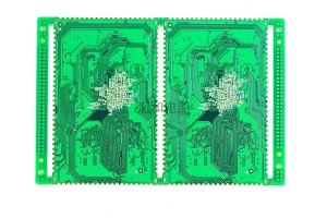
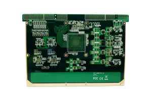
China Wholesale Circuit Board Assembly Pricelist - 8 Layer ENIG via-in-pad PCB – Huihe
The most difficult thing to control the plug hole in the via-in-pad is the solder ball or pad on the ink in the hole. Due to the necessity of using high density BGA (ball grid array) and the miniaturization of SMD chip, the application of in tray hole technology is more and more. Through the reliable through hole filling process, the in plate hole technology can be applied to the design and manufacture of high-density multilayer board, and avoid abnormal welding. Huihe Circuits has been using... -

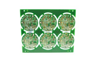
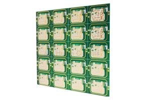
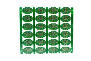
China Wholesale Wifi Pcb Board Suppliers - 6 layer High TG ENIG PCB 10845 – Huihe
Difference between general FR4 and high Tg FR4 The difference between general FR-4 and high FR4-TG lies in the difference of mechanical strength, adhesion, water absorption, dimensional stability, thermal decomposition of hot state (especially after water absorption) under hot state under different conditions (such as thermal expansion). Obviously, high Tg PCB is better than ordinary PCB substrate material. Therefore, in recent years, there is a great demand for high Tg PCB, but the pric... -
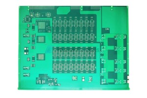
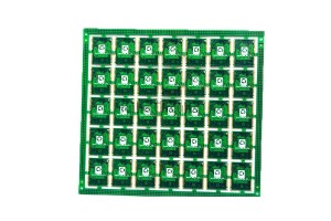
China Wholesale Prototype Pcb Assembly Services Quotes - 16 Layer ENIG Press Fit Hole PCB 31525 – Huihe
About Via-In-Pad PCB The Via-In-Pad PCBs are generally blind holes, which are mainly used to connect the inner layer or the secondary outer layer of HDI PCB with the outer layer, so as to improve the electrical performance and reliability of electronic products, shorten the signal transmission wire, reduce the inductive reactance and capacitive reactance of the transmission line, as well as the internal and external electromagnetic interference. It’s used for conducting. The main problem... -
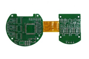
China Wholesale Flexible Pcb Prototype Pricelist - 4 Layer SF302+FR4 Rigid-Flex PCB 19 – Huihe
Points for attention in the design of rigid flexible combination zone 1.The line should transition smoothly, and the direction of the line should be perpendicular to the bending direction. 2.The conductor shall be evenly distributed throughout the bending zone. 3.The width of the conductor shall be maximized throughout the bending zone. 4.PTH design should not be used in rigid flexible transition zone. 5.Bending radius of bending zone of rigid flexible PCB Material of flexible PCB E... -
China Wholesale Bass Filter Circuit Board Pricelist - 8 Layer ENIG via-in-pad PCB 16081 – Huihe
Resin plugging process 1. Definition Resin plugging process refers to the use of resin to plug the buried holes in the inner layer, and then press, which is widely used in high-frequency board and HDI board; it is divided into traditional screen printing Resin Plugging and vacuum resin plugging. Generally, the production process of the product is traditional screen printing resin plug hole, which is also the most common process in the industry. 2. Process Pre process — drilling resin hole — e... -
China Wholesale Single Circuit Board Pricelist - 6 Layer ENIG Impedance Control PCB 9806 – Huihe
About the impedance Impedance is the combination of capacitance and inductance to block the circuit in high frequency signal. Impedance is a kind of AC characteristic, which means that it is related to frequency and is used to describe the high frequency characteristics of PCB. Factors affecting impedance DK (R): determined by raw materials (PCB material, semi cured sheet) Line thickness (T): determined by raw materials and process capability. Line width (W): determined by customer’... -
China Wholesale Gamepad Pcb Factories - 4 Layer Rogers ENIG PCB 25770 – Huihe
Transmission line form in high frequency PCB design Both transmission lines and waveguides can be used as carriers for high frequency signal transmission, while microstrip lines and strip lines in TEM transmission lines and Substrate Integrated Waveguide in Waveguide structures are applied in the design of high frequency PCBs. High frequency PCB wiring skills The radiation intensity of the signal is proportional to the wiring length of the signal line. The longer the high-frequency ... -
China Wholesale Pcb Producer Pricelist - 6 layer ENIG impedance control PCB 16403 – Huihe
About Multilayer PCB With the increasing complexity of circuit design, in order to increase the area of wiring, multilayer PCB can be used. Multilayer board is a PCB that contains multiple working layers. In addition to the top and bottom layers, it also includes signal layer, middle layer, internal power supply and ground layer. The number of layers of PCB represents that there are several independent wiring layers. Generally, the number of layers is even and includes the outermost two ... -
China Wholesale Ic Circuit Board Pricelist - 4 Layer FR4+Rogers PCB 29166 – Huihe
About High-frequency mixed-voltage PCB High-frequency mixed-voltage circuit boards are pressed using different laminated materials to optimize electrical performance and improve system reliability. The biggest challenge in manufacturing this type of high frequency PCB is to match the thermal expansion coefficient (CTE) of the different materials to fit the PCB manufacturing and component assembly. Typically, such circuit designs include a combination of FR-4 materials and PTFE laminated ... -
China Wholesale Printed Circuit Fabrication Pricelist - 8 Layer ENIG Impedance Control PCB 16978 – Huihe
Deficiencies of the blind buried vias The main problem of blind buried via is the high cost. In contrast, buried holes cost less than blind holes, but the use of both types of holes can significantly increase the cost of a board. The cost increase is due to the more complex manufacturing process of the blind buried hole, that is, the increase in manufacturing processes also leads to the increase in testing and inspection processes. Buried Via Buried vias are used to connect differen... -
China Wholesale Flex Pcb Pricelist - 6 Layer ENIG via-in-pad PCB 16842 – Huihe
The advantages and disadvantages of plugging and no plugging? In terms of plug holes, they have the following advantages 1. the plug hole can prevent PCB through the wave soldering tin from the through hole through the component surface caused by short circuit; That is to say, within the scope of the wave soldering design area (generally the welding surface is 5mm or above) there is no hole or hole to do plug hole treatment. 2. The plug hole protects against possible short circuits caused by ...


