-
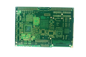
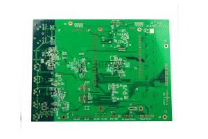
China Wholesale Soldering Pcb Components Pricelist - 14 Layer Blind Buried Via PCB – Huihe
About Blind Buried Via PCB Blind vias and buried vias are two ways to establish connections between layers of printed circuit board. The blind vias of the printed circuit board are copper-plated vias that can be connected to the outer layer through most of the inner layer. The burrow connects two or more inner layers but does not penetrate the outer layer. Use microblind vias to increase line distribution density, improve radio frequency and electromagnetic interference, heat conduction,... -
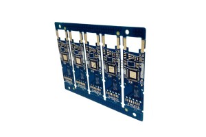
China Wholesale Round Circuit Board Manufacturers - 4 Layer ENIG impedance half hole PCB 13633 – Huihe
Half hole splicing mode By using the stamp hole splicing method, the purpose is to make the connecting bar between the small plate and the small plate. In order to facilitate the cutting, some holes will be opened on the top of the bar (the diameter of the conventional hole is 0.65-0.85 MM), which is the stamp hole. Now the board has to pass the SMD machine, so when you do the PCB, you can connect the board too many PCB. at a time After the SMD, the back board should be separated, and th... -
China Wholesale Rigid Flex Circuit Boards Quotes - 2 Layer in spray half hole PCB 14146 – Huihe
About metallizing half-hole PCB Metal half hole (groove) is a hole after the hole after the second drilling, shape process, and finally retain the metal hole (groove) half, simply said that the plate edge metallized hole cut half, the plate edge semi-metallic hole process is a very mature process. How to control the product quality after forming the semi-metallic hole on the edge of the plate. Such as hole wall copper prickle, residual has been a difficult process. A full row of semi-met... -
China Wholesale Mp5 Circuit Board Factories - 2 Layer F4B OSP PCB – Huihe
Effect of different types of copper foil on electrical properties In the design of high-frequency PCB, designers usually pay more attention to the dielectric constant (DK) and tangent loss (DF) of PCB when selecting materials, and only pay attention to the thickness of copper foil when selecting copper foil, which is easy to ignore the influence of different types of copper foil roughness on the electrical properties of products. SEM analysis of the micro morphology of different types of copp... -
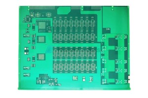
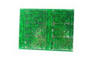
China Wholesale Flexible Pcb Prototype Quotes - 16 Layer ENIG Press Fit Hole PCB 31525 – Huihe
About Via-In-Pad PCB The Via-In-Pad PCBs are generally blind holes, which are mainly used to connect the inner layer or the secondary outer layer of HDI PCB with the outer layer, so as to improve the electrical performance and reliability of electronic products, shorten the signal transmission wire, reduce the inductive reactance and capacitive reactance of the transmission line, as well as the internal and external electromagnetic interference. It’s used for conducting. The main problem... -

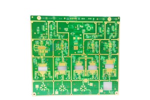
China Wholesale Rf Pcb Pricelist - 6 Layer Rogers+ FR4 PCB – Huihe
The electrical, thermal and mechanical properties of high-frequency materials are different from those of conventional FR-4 materials. High frequency PCB has low dielectric constant Dk, low transmission delay, low loss factor Df and low dielectric loss. The high-frequency microwave board and RF board produced by Huihe Circuit include 5G base station antenna circuit board, 4G intermodulation antenna circuit board, high-precision impedance circuit board, high-frequency high-speed mixed voltage ... -
China Wholesale Printed Circuit Board Components Quotes - 4 Layer FR4+Rogers PCB 29166 – Huihe
About High-frequency mixed-voltage PCB High-frequency mixed-voltage circuit boards are pressed using different laminated materials to optimize electrical performance and improve system reliability. The biggest challenge in manufacturing this type of high frequency PCB is to match the thermal expansion coefficient (CTE) of the different materials to fit the PCB manufacturing and component assembly. Typically, such circuit designs include a combination of FR-4 materials and PTFE laminated ... -
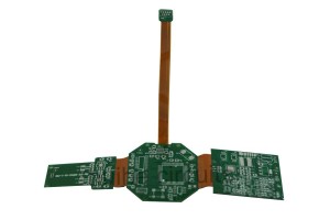
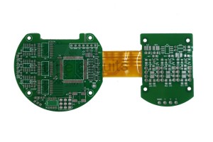
China Wholesale Ims Pcb Factories - 4 Layer FPC+FR4 Rigid-Flex PCB – Huihe
About the Rigid-Flex PCB Rigid-Flex PCB, is the flexible PCB and traditional Rigid PCB, after many procedures, according to the relevant process requirements combined together, forming at the same time with FPC characteristics and PCB characteristics of the circuit board. It can be used in some products with special requirements, both a certain flexible area and a certain rigid area, to save the internal space of the product, reduce the volume of finished products, improve the performance of ... -
China Wholesale Pcb Circuit Manufacturers - 4 Layer SF302+FR4 Rigid-Flex PCB 19 – Huihe
Points for attention in the design of rigid flexible combination zone 1.The line should transition smoothly, and the direction of the line should be perpendicular to the bending direction. 2.The conductor shall be evenly distributed throughout the bending zone. 3.The width of the conductor shall be maximized throughout the bending zone. 4.PTH design should not be used in rigid flexible transition zone. 5.Bending radius of bending zone of rigid flexible PCB Material of flexible PCB E... -
China Wholesale Surface Mount Prototype Board Factories - 6 Layer ENIG Impedance Control PCB 7201 – Huihe
PCB impedance line design 1.In the process of PCB LAYOUT, consider the basic conditions required to control the impedance are: line width, line distance, line length, impedance line shielding reference layer, according to these requirements will be placed in the appropriate position of the impedance line. 2. The shielding reference layer preferentially selects the line adjacent to the layer where the impedance line is located. The corresponding position of the impedance line is a complete cop... -
China Wholesale Flex Pcb Prototyping Manufacturers - 12 layer impedance Control HASL PCB – Huihe
Why choose us? 1.Precision technology: it can process all kinds of high precision and high difficulty PCB, with 28 layers and 3 / 3mil line spacing 2.Professional Customization: to undertake proofing, batch PCB order demand 3.Advanced equipment: automatic copper deposition / electroplating line, LDI / CCD exposure machine and other equipment to produce high quality and high reliability products Our advantage As a professional PCB manufacturer, Huihe Circuits Co., Ltd. focuses on th... -

China Wholesale Prototype Pcb Suppliers - 6 layer ENIG Impedance Control Heavy Copper PCB 15881 – Huihe
Functions of heavy copper PCB Heavy copper PCB has the best extension functions, is not limited by the processing temperature, high melting point can be used oxygen blowing, low temperature at the same brittle and other hot melt welding, but also fire prevention, belongs to the non-combustible material. Even in highly corrosive atmospheric conditions, copper sheets form a strong, non-toxic passivation protective layer. Difficulty in machining control of heavy copper PCB Thickness of copper PC...


