
China Wholesale Double Sided Pcb Board Prototype Factories - 14 Layer Blind Buried Via PCB – Huihe
China Wholesale Double Sided Pcb Board Prototype Factories - 14 Layer Blind Buried Via PCB – Huihe Detail:
About Blind Buried Via PCB
Blind vias and buried vias are two ways to establish connections between layers of printed circuit board. The blind vias of the printed circuit board are copper-plated vias that can be connected to the outer layer through most of the inner layer. The burrow connects two or more inner layers but does not penetrate the outer layer. Use microblind vias to increase line distribution density, improve radio frequency and electromagnetic interference, heat conduction, applied to servers, mobile phones, digital cameras.
Buried Vias
The buried Vias connects two or more inner layers but does not penetrate the outer layer
|
|
Min. Hole Diameter/mm |
Minimum ring/mm |
via-in-pad Diameter/mm |
Maximum Diameter/mm |
Aspect Ratio |
|
Blind Vias(conventional) |
0.1 |
0.1 |
0.3 |
0.4 |
1:10 |
|
Blind Vias (special product) |
0.075 |
0.075 |
0.225 |
0.4 |
1:12 |
Blind Vias
Blind Vias is to connect an outer layer to at least one inner layer
|
|
Min. Hole Diameter/mm |
Minimum ring/mm |
via-in-pad Diameter/mm |
Maximum Diameter/mm |
Aspect Ratio |
|
Blind Vias(mechanical drilling) |
0.1 |
0.1 |
0.3 |
0.4 |
1:10 |
|
Blind Vias (Laser drilling) |
0.075 |
0.075 |
0.225 |
0.4 |
1:12 |
Equipment display

Automatic Plating Line

PTH line

LDI

CCD Exposure Machine
The advantage of blind Vias and buried Vias for engineers is the increase of component density without increasing layer number and size of circuit board. For electronic products with narrow space and small design tolerance, blind hole design is a good choice. The use of such holes helps the circuit design engineer to design a reasonable hole/pad ratio to avoid excessive ratios.
Application

Communications

Security electronics

Railtransit
Our factory


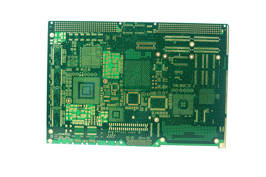
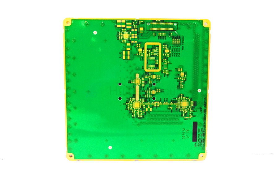
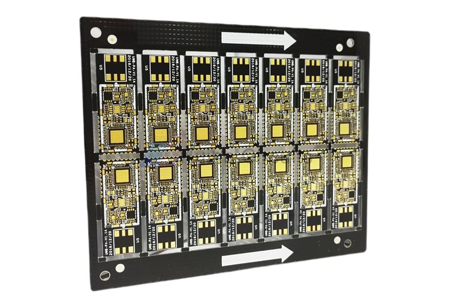
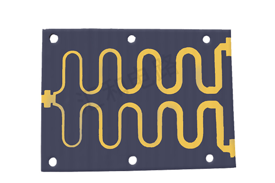
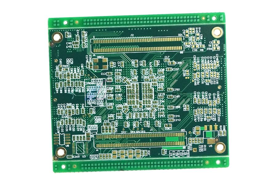
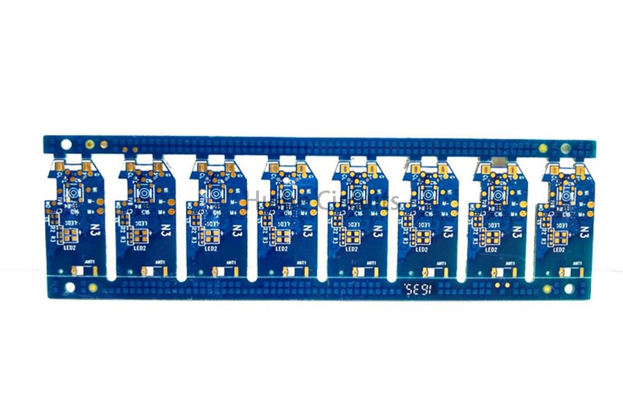
Product detail pictures:


Related Product Guide:
Our personnel are always in the spirit of "continuous improvement and excellence", and with the superior quality products, favorable price and good after-sales services, we try to win every customer's trust for China Wholesale Double Sided Pcb Board Prototype Factories - 14 Layer Blind Buried Via PCB – Huihe , The product will supply to all over the world, such as: St. Petersburg, Latvia, Montreal, We set a strict quality control system. We have return and exchange policy, and you can exchange within 7 days after receive the wigs if it is in new station and we service repairing free for our products. Please feel free to contact us for further information and we will offer you competitive price list then.
The goods are very perfect and the company sales manager is warmful, we will come to this company to purchase next time.
-
China Wholesale Incubator Circuit Board Manufac...
-
China Wholesale Pcba Circuit Board Manufacturer...
-

China Wholesale Ssd Pcb Factories - 4 Layer FR...
-
China Wholesale Rf Circuit Board Factories - 2...
-
China Wholesale Sensor Circuit Board Pricelist ...
-
China Wholesale Custom Circuit Board Printing F...


