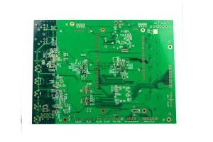
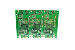
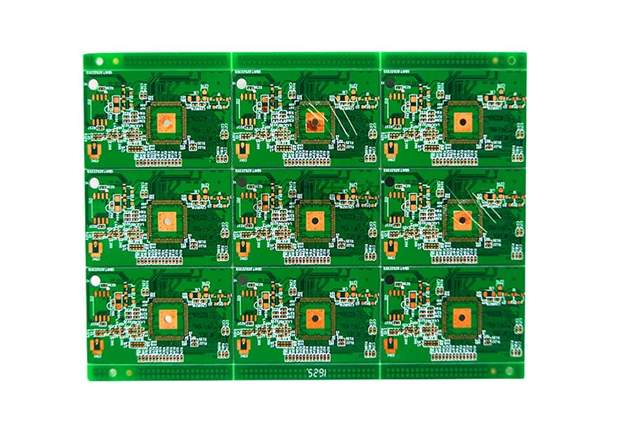
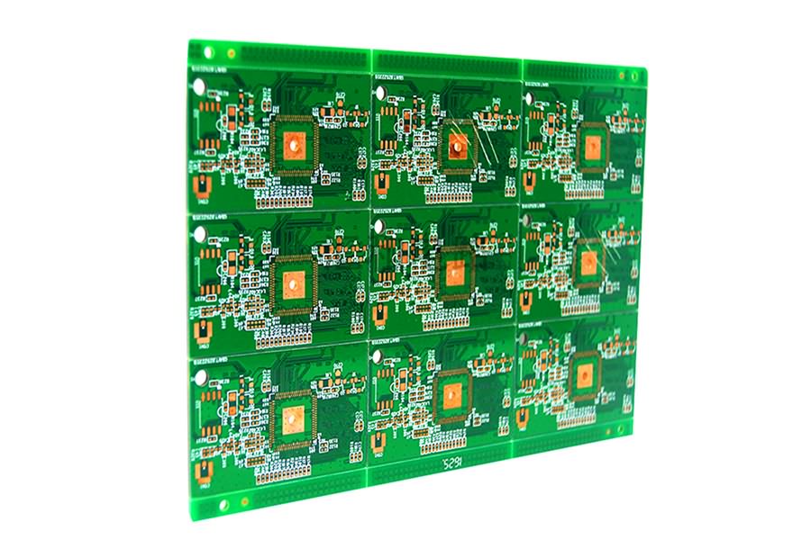
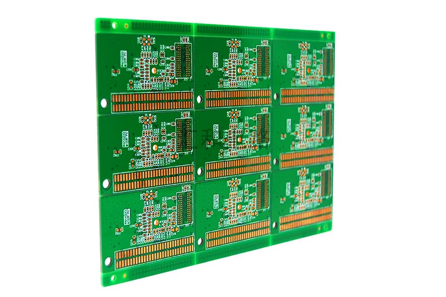
4 Layer FR4 OSP Impedance Control PCB

Characteristic Impedance Control PCB
The characteristic impedance of the conductor on the PCB is an important index of circuit design, especially in the PCB design of high frequency circuit, we must consider whether the characteristic impedance of the conductor is consistent with the characteristic impedance required by the device or signal.
PCB Impedance Matching
In the PCB, if there is a signal transmission, it is expected to be from the sending end of the power supply, in the case of minimum energy loss, can be smoothly transmitted to the receiving end, and the receiving end will be completely absorbed without any reflection. To achieve this transmission, the impedance in the line must be equal to the impedance inside the originating end for it to be called impedance matching. Impedance matching is one of the design elements when designing high speed PCB circuit. The impedance value is absolutely related to the routing mode.
For example, whether you walk on a surface layer (Microstrip) or an inner layer (Stripline/Double Stripline), distance from the reference power layer or layer, route width, PCB material, etc., all affect the characteristic impedance value of the route. That is to say, the impedance value can only be determined after wiring, and the characteristic impedance produced by different PCB manufacturers also varies slightly. Generally, the simulation software will be unable to take into account some impedance discontinuous wiring due to the limitation of the line model or the mathematical algorithm used.
At this time, only some Temninators can be reserved on the schematic diagram, such as series resistance, to mitigate the discontinuous effect of the wiring impedance. The real fundamental solution to the problem is to try to avoid the occurrence of impedance discontinuity when wiring.
Equipment Display

PCB Automatic Plating Line

PCB PTH Line

PCB LDI

PCB CCD Exposure Machine
Factory Show

PCB Manufacturing Base

Admin Receptionist

Meeting Room