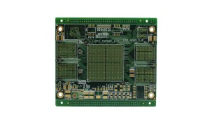
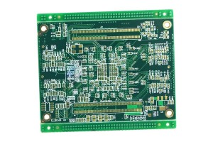
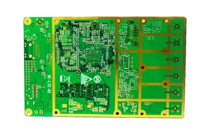
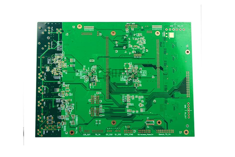
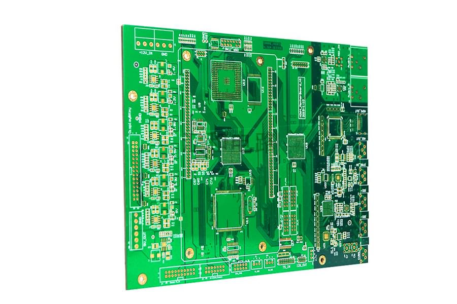
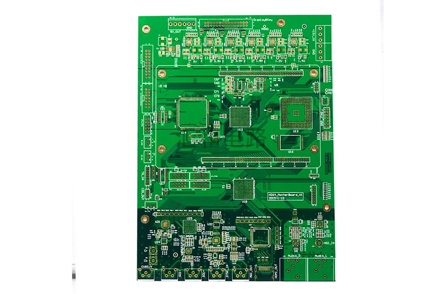
6 Layer FR4 ENIG Impedance Control PCB
PCB Impedance Line Design
1.In the process of PCB LAYOUT, consider the basic conditions required to control the impedance are: line width, line distance, line length, impedance line shielding reference layer, according to these requirements will be placed in the appropriate position of the impedance line.
2. The shielding reference layer preferentially selects the line adjacent to the layer where the impedance line is located. The corresponding position of the impedance line is a complete copper sheet, so as to ensure that the deviation of the impedance value is controllable. In actual production, according to the LAYOUT design, the nearest copper sheet to the impedance line is selected as the reference layer. If there is no copper sheet in the corresponding position, the impedance cannot be controlled. If the copper sheet cannot completely shield the impedance line, the impedance deviation is uncontrollable.
3, The distribution of impedance line special attention: the characteristic impedance is only a single line, only need to consider the line width and the length of the line. Differential impedances must consist of two lines of the same line width completely parallel to each other. Coplanar impedance is the interaction between the line and the ground copper, so the line width needs to be the same, both sides of the line are surrounded by the ground copper, and the distance from the line to the ground copper is exactly the same from beginning to end.
What Is Impedance Control On The PCB Used For?
Controlled impedance is preferred when the signal must have a certain impedance to work properly. In high frequency applications, a constant impedance must be maintained throughout the board to ensure the integrity of the transmitted data and the clarity of the signal. The longer the conductor path or the higher the frequency, the more adjustment is required. Lack of rigor at this level can increase the switching time of an electronic device or circuit and lead to unexpected errors.
Uncontrolled impedance is difficult to analyze after the components are assembled on the circuit. Components have different tolerance ranges depending on the lot. In addition, their characteristics can be affected by temperature fluctuations, which can lead to malfunctions. In this case, replacing the component seems to be the solution, but in fact it is the insufficient impedance of the conductor wiring that is the problem.
Therefore, PCB design must check the conductor wiring impedance and its tolerance in advance to ensure that the component values meet the requirements.
Factory Show

PCB Manufacturing Base

Admin Receptionist

Meeting Room