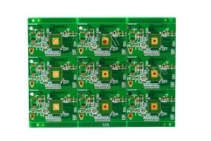
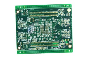
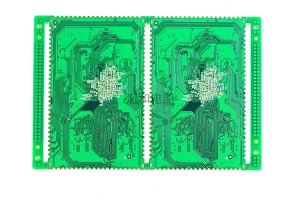
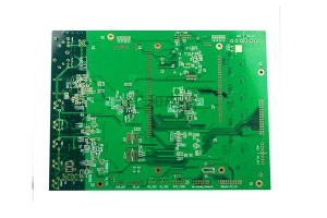
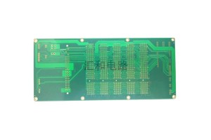
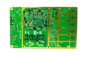
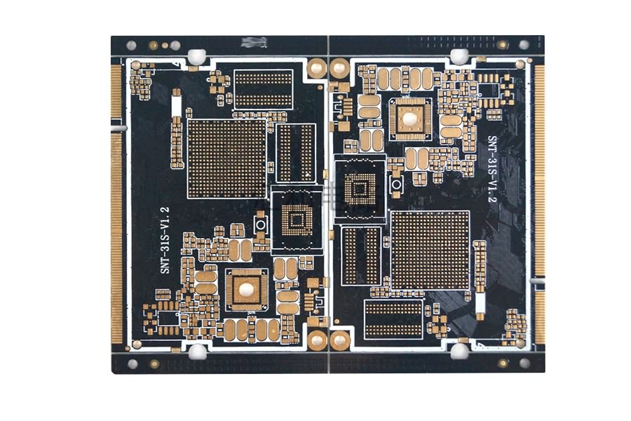
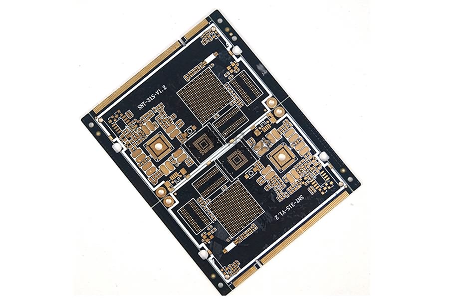
6 Layer FR4 ENIG Impedance Control PCB

Factors Determining Controlled Impedance
The characteristic impedance of a PCB is usually determined by its inductance and capacitance, resistance and conductance. These factors are functions of the physical size of the circuit, the dielectric constant and dielectric thickness of the PCB substrate material. In general, the line impedance of a PCB ranges from 25 to 125Ω. The PCB structure that determines the impedance value consists of the following factors:
Width and thickness of top and bottom copper signal lines
Width of top and bottom copper wires. The inner layer process range of the assembly and circuit is 0.5oz 3/3mil to 6oz 15/12mil copper signal line, and the outer line distance varies from 1/3oz 3/3mil to 6oz 15/12mil.
Core plate or semi-cured sheet thickness on both sides of copper wire
The semi-cured sheet is used as a bonding layer to hold all core boards together in a PCB. When designing the impedance control PCB, the thickness of the semi-cured sheet on both sides of the core board should be the same.
Dielectric constant of core PCB and semi-cured sheet
If the dielectric constant of the core plate and the semi-cured sheet are different, the impedance will also change. Therefore, the dielectric constant of the two should be the same.
Equipment Display

Automatic Plating Line

PTH Line

LDI