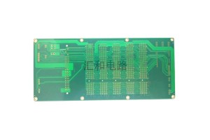
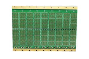
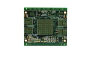
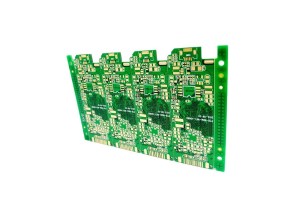
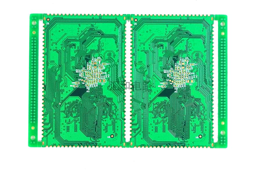
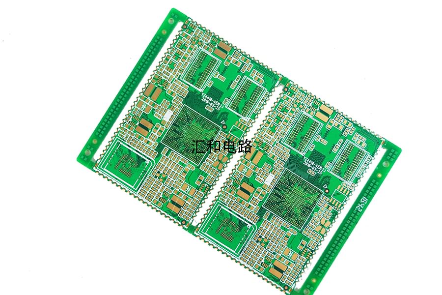
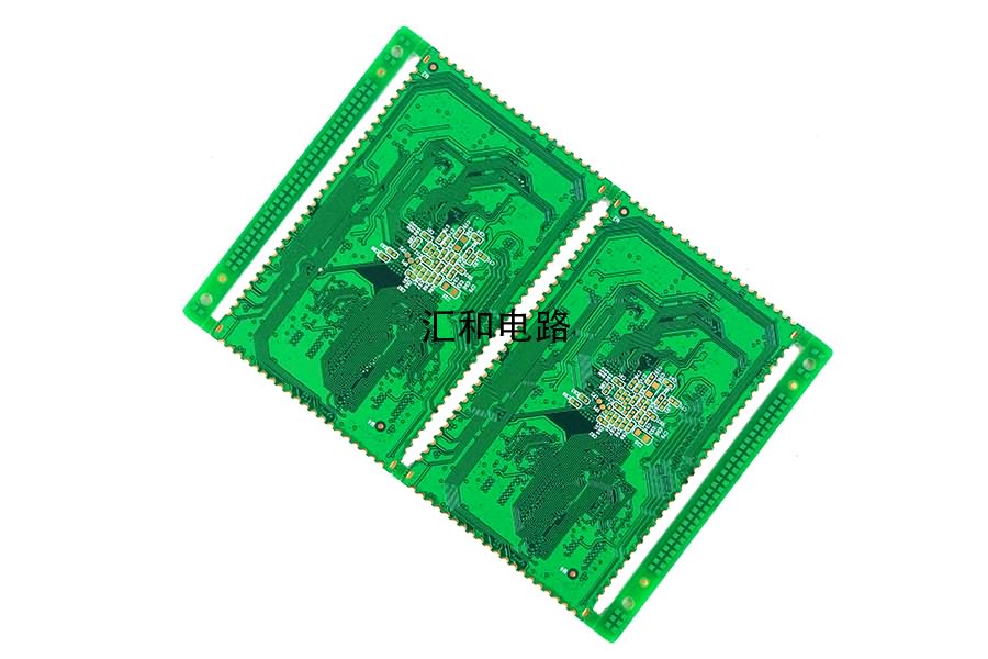
6 Layer FR4 ENIG Impedance Control PCB

About The Impedance
Impedance is the combination of capacitance and inductance to block the circuit in high frequency signal. Impedance is a kind of AC characteristic, which means that it is related to frequency and is used to describe the high frequency characteristics of PCB.
Factors Affecting Impedance
DK (R): determined by raw materials (PCB material, semi cured sheet)
Line Thickness (T): determined by raw materials and process capability.
Line Width (W): determined by customer’s original design and process capability.
Medium thickness (H): determined by the customer’s original design, process capability and raw materials.
Therefore, in the design of PCB, we must control the impedance of the wiring on the board, so as to avoid the signal reflection and other electromagnetic interference and signal integrity problems as far as possible, and ensure the stability of the actual use of PCB.
Equipment Display

PCB Automatic Plating Line

PCB PTH Line

PCB LDI