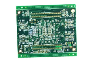
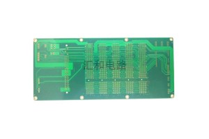
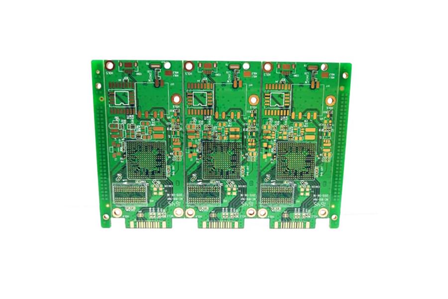
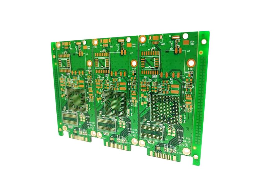
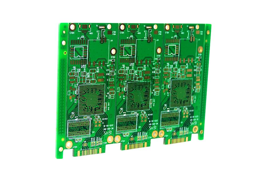
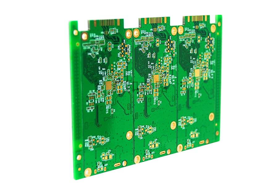
4 Layer FR4 ENIG Impedance Control PCB

Impedance Control PCB
In the case of transmission of high frequency signals, the controlled impedance helps to ensure that the signal does not decay significantly during transmission. In essence, controlled impedance refers to the matching of the material properties of the substrate to the characteristics of the line/dielectric layer to ensure that the impedance value of the line signal is within the tolerance of the reference value. Controlled impedance PCBs provide reliable and consistent high frequency characteristics.
Applications Of The Impedance Control PCB
Internet box, TV, video game, digital camera, GPS
Analog and digital telecommunications
Computers, tablets, cell phones
Video signal processing
Motor control module
Relationship Between Characteristic Impedance Factors
From the perspective of PCB manufacturing, the key factors that affect the impedance are as follows:
- Line width (W), the impedance decreases with the increase of linewidth.
- Line distance (s), the impedance increases with the increase of distance.
-Line thickness (T), the impedance decreases with the increase of line thickness.
- Dielectric thickness (H), the greater the dielectric thickness, the greater the impedance.
- Dielectric constant (DK), the higher the dielectric constant, the smaller the impedance.
Equipment Display

PCB Automatic Plating Line

PCB PTH Line

PCB LDI

PCB CCD Exposure Machine
Factory Show

PCB Manufacturing Base

Admin Receptionist

Meeting Room