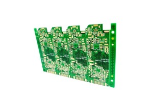
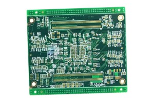
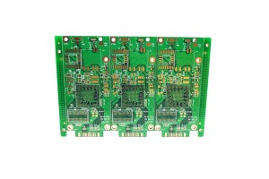
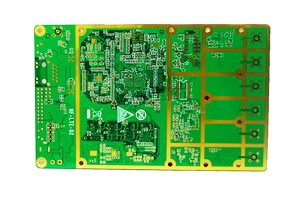
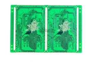
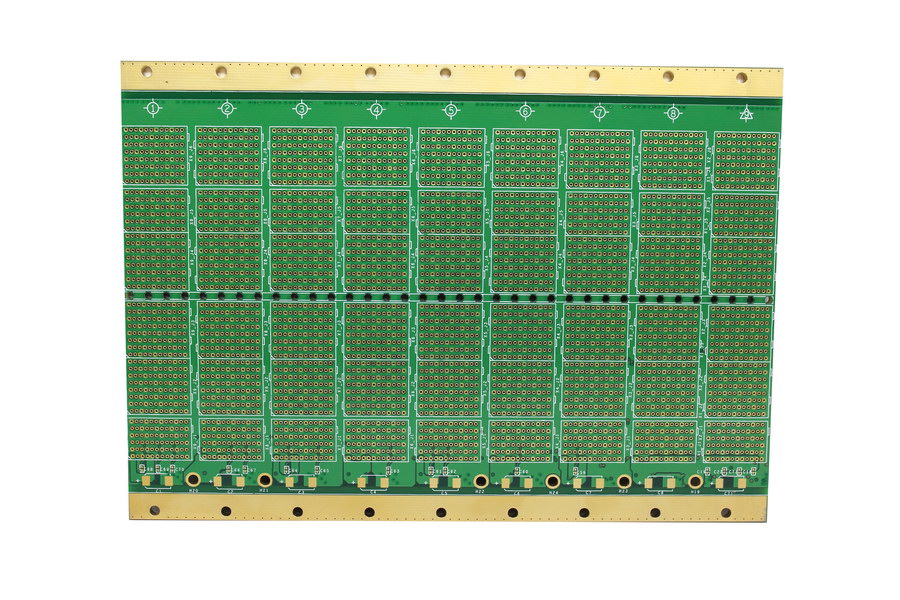
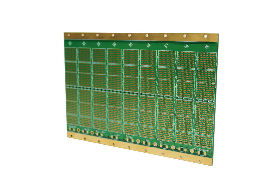
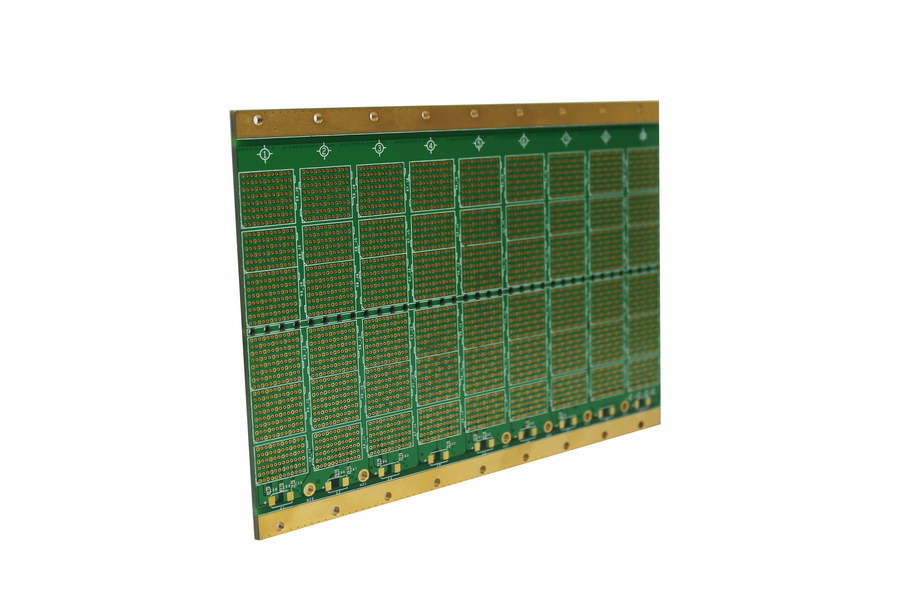
12 Layer FR4 ENIG Impedance Control PCB
Why do PCB boards need impedance?
1. PCB circuit board to consider the insertion and installation of electronic components, later SMT patch insertion also need to consider the conductivity and signal transmission performance and other issues, so it will require the impedance as low as possible.
2. PCB circuit board in the production process of copper deposition, tin plating (or electroless plating, hot spray tin), soldering and other processes, the materials used must require low resistivity, to ensure that the overall impedance value of the circuit board to meet the product quality requirements, in order to operate normally.
3. PCB circuit board tin plating is the most prone to problems in the whole circuit board production, is the key link affecting the impedance; its biggest defect is easy oxidation or deliquescence, poor brazing, so that the circuit board is difficult to solder, impedance is too high, resulting in poor conductivity or unstable performance of the whole board.
4. The conductor in the PCB circuit board will have a variety of signal transmission, the line itself due to etching, laminate thickness, wire width and other factors, will cause the impedance value change, make the signal distortion, leading to the performance of the circuit board decline, so it is necessary to control the impedance value in a certain range.