-
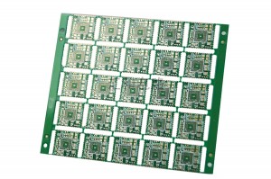
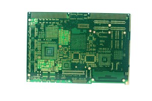
China Wholesale Panel Circuit Board Pricelist - 4 Layer ENIG half hole PCB 12026 – Huihe
Difficulties in machining metallized half-hole PCB Metalized half-hole PCB after forming the hole wall copper black, burr residual, deviation has been a difficult problem in the molding process of PCB factory. Especially the whole row of half holes similar to stamp holes, the aperture is about 0.6 mm, the hole wall spacing is 0.45 mm, the outer figure spacing is 2 mm, because the spacing is very small, it is easy to cause short circuit because of copper skin. The general metallized half-hole ... -
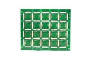
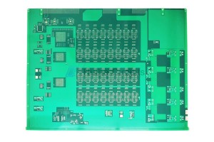
China Wholesale Ims Pcb Suppliers - 4 Layer ENIG half hole PCB – Huihe
Difficulties in machining metallized half-hole PCB Metalized half-hole PCB after forming the hole wall copper black , burr residuadeviation has been a difficult problem in the molding process of PCB factoEspecially the whole row of half holes similar to stamp holes , the aperture isabout 0.6 mm , the hole wall spacing is 0 . 45 mm , the outer figure spacing is 2mm , because the spacing is very small , it is easy to cause short circuitbecause of copper skin. The general metallized half-ho... -
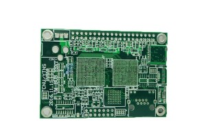
China Wholesale Pcb Bare Board Quotes - 10 Layer Medium TG Gold Finger PCB – Huihe
The advantages of high Tg materials The main advantage of high Tg materials is higher operating temperature( MOT ) , which can carry more current . According to experience , TG minusabout 20 C can be used as mot . At this temperature , the PCB can runnormally for a long time without damage. The heat resistance temperature of the common solder mask is usually lowerthan the Tg of the substrate . The conventional maximum operatingtemperature of solder mask is about 150 C . For high Tg appli... -
China Wholesale Pcba Circuit Board Quotes - 6 Layer HASL Blind Buried Via PCB 13699 – Huihe
Features of the Buried Via The manufacturing process cannot be achieved by drilling after bonding. Drilling must be performed at individual circuit layers. The inner layer must be partially bonded first, followed by electroplating treatment, and then all bonded finally. This process is usually used only on high-density PCBs to increase the available space for other circuit layers The basic process of making HDI blind buried Via PCB Equipment display Automatic Plating Lin... -
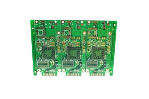
China Wholesale Double Sided Pcb Pricelist - 14 Layer Blind Buried Via PCB – Huihe
About Blind Buried Via PCB Blind vias and buried vias are two ways to establish connections between layers of printed circuit board. The blind vias of the printed circuit board are copper-plated vias that can be connected to the outer layer through most of the inner layer. The burrow connects two or more inner layers but does not penetrate the outer layer. Use microblind vias to increase line distribution density, improve radio frequency and electromagnetic interference, heat conduction,... -

China Wholesale Round Pcb Board Manufacturers - 6 Layer ENIG Impedance Control PCB 10222 – Huihe
Factors determining controlled impedance The characteristic impedance of a PCB is usually determined by its inductance and capacitance, resistance and conductance. These factors are functions of the physical size of the circuit, the dielectric constant and dielectric thickness of the PCB substrate material. In general, the line impedance of a PCB ranges from 25 to 125Ω. The PCB structure that determines the impedance value consists of the following factors: Width and thickness of top and... -
China Wholesale Prototype Pcb Board Quotes - 16 Layer ENIG Press Fit Hole PCB 31525 – Huihe
About Via-In-Pad PCB The Via-In-Pad PCBs are generally blind holes, which are mainly used to connect the inner layer or the secondary outer layer of HDI PCB with the outer layer, so as to improve the electrical performance and reliability of electronic products, shorten the signal transmission wire, reduce the inductive reactance and capacitive reactance of the transmission line, as well as the internal and external electromagnetic interference. It’s used for conducting. The main problem... -
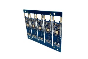
China Wholesale Drc Pcb Factories - 4 Layer ENIG impedance half hole PCB 13633 – Huihe
Half hole splicing mode By using the stamp hole splicing method, the purpose is to make the connecting bar between the small plate and the small plate. In order to facilitate the cutting, some holes will be opened on the top of the bar (the diameter of the conventional hole is 0.65-0.85 MM), which is the stamp hole. Now the board has to pass the SMD machine, so when you do the PCB, you can connect the board too many PCB. at a time After the SMD, the back board should be separated, and th... -
China Wholesale Teflon Pcb Board Manufacturers - 6 Layer ENIG Impedance Control PCB 7736 – Huihe
Why PCB to do impedance? PCB impedance refers to the resistance and the parameters of the reactance, which acts as a barrier to the alternating current. Impedance processing is essential in PCB. Here’s why: 1, PCB to consider the plug installation of electronic components, SMT patch plug also needs to consider the conductivity and signal transmission performance, so it will require the lower the impedance, the better. 2, PCB in the production process through copper deposition, electroplating ... -
China Wholesale Power Supply Pcb Board Pricelist - 2 layer ENIG Heavy Copper PCB 15872 – Huihe
Difficulties in drilling heavy copper PCBs With the increase of the copper thickness, the thickness of the heavy copper PCB also increases. heavy copper PCB is usually more than 2.0mm thick, drilling production due to the thickness of the thickness of the plate and copper thick factors, production is more difficult. In this regard, the use of a new cutter, reduce the service life of the drill cutter, section drilling has become an effective solution to the heavy copper PCB drilling. In a... -
China Wholesale Ssd Pcb Quotes - 4 Layer ENIG Impedance Control PCB 9115 – Huihe
About the impedance control In the case of transmission of high frequency signals, the controlled impedance helps to ensure that the signal does not decay significantly during transmission. In essence, controlled impedance refers to the matching of the material properties of the substrate to the characteristics of the line/dielectric layer to ensure that the impedance value of the line signal is within the tolerance of the reference value. Controlled impedance PCBs provide reliable and c... -

China Wholesale Custom Pcb Board Manufacturers - 8 layer ENIG Impedance Control Heavy Copper PCB 16555 – Huihe
Thin core heavy copper PCB copper foil choice The most concerned problem of heavy copper CCL PCB is the pressure resistance problem, especially the thin core heavy copper PCB (thin core is medium thickness ≤ 0.3mm), the pressure resistance problem is particularly prominent, thin core heavy copper PCB will generally choose RTF copper foil for production, RTF copper foil and STD copper foil main difference is the length of the wool Ra is different, RTF copper foil Ra is significantly less ...


