-
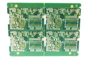
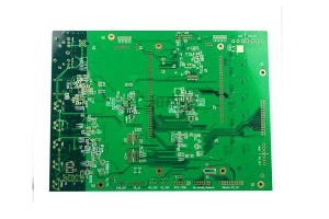
China Wholesale Mp5 Circuit Board Manufacturers - 10 Layer ENIG Blind Vias PCB 28526 – Huihe
About Blind Buried Via PCB Blind Via: which enables the connection and conduction between the inner and outer layers Buried Via: which can connect and guide between inner layers Blind Vias are mostly small holes with a diameter of 0.05mm~0.15mm. There are laser hole forming, plasma etched hole and photoinduced hole forming, and laser hole forming is usually used. HDI: High-density interconnection, non-mechanical drilling, micro-blind hole ring below 6mil, inside and outside layers of wiring l... -
China Wholesale Microwave Pcb Manufacturers - 10 Layer ENIG Blind Vias PCB 28526 – Huihe
About Blind Buried Via PCB Blind Via: which enables the connection and conduction between the inner and outer layers Buried Via: which can connect and guide between inner layers Blind Vias are mostly small holes with a diameter of 0.05mm~0.15mm. There are laser hole forming, plasma etched hole and photoinduced hole forming, and laser hole forming is usually used. HDI: High-density interconnection, non-mechanical drilling, micro-blind hole ring below 6mil, inside and outside layers of wiring l... -
China Wholesale Cpu Pcb Pricelist - 10 Layer Impedance Control Resin Plugging PCB 3 – Huihe
The difference between electroplating plug hole and resin plug hole 1. Surface difference: The electroplating plug hole is filled by copper plating, and the inner surface of the hole is full of metal. The resin plug hole is filled with epoxy resin after copper plating on the hole wall, and finally copper plating on the resin surface. The effect is that the hole can be conducted, and there is no dent on the surface, which does not affect the welding. 2. The process is different Electroplating ... -
China Wholesale Flex Printed Circuit Factories - 4 layer Taconic ENIG PCB 53 – Huihe
About PTFE PCB PTFE (commonly known as Teflon) is an ideal dielectric for RF applications, but it is not easily compatible with the conventional dielectric FR4 in PCB manufacturing. Ceramic dielectric is the most commonly used dielectric material in multilayer PCB. It can be used as a separate dielectric layer in special applications and as an inner dielectric layer in FR4 laminated structure in conventional applications. Many RF signal layers of RF design have large non copper filled ar... -
China Wholesale Multisim Pcb Quotes - 2 Layer in spray half hole PCB 14146 – Huihe
About metallizing half-hole PCB Metal half hole (groove) is a hole after the hole after the second drilling, shape process, and finally retain the metal hole (groove) half, simply said that the plate edge metallized hole cut half, the plate edge semi-metallic hole process is a very mature process. How to control the product quality after forming the semi-metallic hole on the edge of the plate. Such as hole wall copper prickle, residual has been a difficult process. A full row of semi-met... -
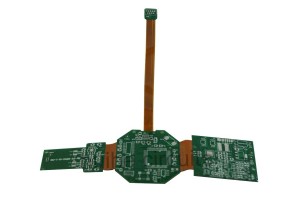
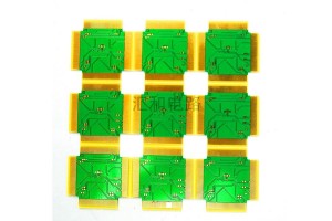
China Wholesale Ptfe Pcb Manufacturers - 4 Layer FPC+FR4 Rigid-Flex PCB – Huihe
About the Rigid-Flex PCB Rigid-Flex PCB, is the flexible PCB and traditional Rigid PCB, after many procedures, according to the relevant process requirements combined together, forming at the same time with FPC characteristics and PCB characteristics of the circuit board. It can be used in some products with special requirements, both a certain flexible area and a certain rigid area, to save the internal space of the product, reduce the volume of finished products, improve the performance of ... -
China Wholesale Mini Pcb Board Suppliers - 2 layer High TG ENIG PCB 11590 – Huihe
About High Tg material Tg is the mechanical property that specifies the glass transition temperature, the maximum temperature at which the glass remains rigid.Normal PCB FR4-TG is 130-140 degrees, medium TG is greater than 150-160 degrees, high TG is greater than 170 degrees. Compared with standard FR4, high FR4-TG has better mechanical and chemical heat resistance and moisture resistance.The higher the Tg value, the better the heat resistance of the material, so, especially in the lead-... -
China Wholesale Matte Black Pcb Suppliers - 4 Layer ENIG half hole PCB – Huihe
Difficulties in machining metallized half-hole PCB Metalized half-hole PCB after forming the hole wall copper black , burr residuadeviation has been a difficult problem in the molding process of PCB factoEspecially the whole row of half holes similar to stamp holes , the aperture isabout 0.6 mm , the hole wall spacing is 0 . 45 mm , the outer figure spacing is 2mm , because the spacing is very small , it is easy to cause short circuitbecause of copper skin. The general metallized half-ho... -
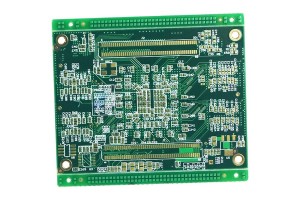
China Wholesale Printed Circuit Board Assembly Quotes - 16 Layer ENIG Press Fit Hole PCB 31525 – Huihe
About Via-In-Pad PCB The Via-In-Pad PCBs are generally blind holes, which are mainly used to connect the inner layer or the secondary outer layer of HDI PCB with the outer layer, so as to improve the electrical performance and reliability of electronic products, shorten the signal transmission wire, reduce the inductive reactance and capacitive reactance of the transmission line, as well as the internal and external electromagnetic interference. It’s used for conducting. The main problem... -
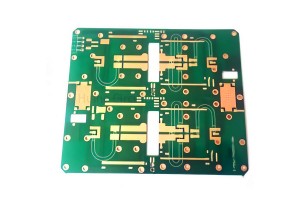
China Wholesale Euro Pcb Manufacturers - 6 Layer ENIG Impedance Control PCB 7201 – Huihe
PCB impedance line design 1.In the process of PCB LAYOUT, consider the basic conditions required to control the impedance are: line width, line distance, line length, impedance line shielding reference layer, according to these requirements will be placed in the appropriate position of the impedance line. 2. The shielding reference layer preferentially selects the line adjacent to the layer where the impedance line is located. The corresponding position of the impedance line is a complete cop... -
China Wholesale Ims Pcb Suppliers - 12 layer impedance Control HASL PCB – Huihe
Why choose us? 1.Precision technology: it can process all kinds of high precision and high difficulty PCB, with 28 layers and 3 / 3mil line spacing 2.Professional Customization: to undertake proofing, batch PCB order demand 3.Advanced equipment: automatic copper deposition / electroplating line, LDI / CCD exposure machine and other equipment to produce high quality and high reliability products Our advantage As a professional PCB manufacturer, Huihe Circuits Co., Ltd. focuses on th... -
China Wholesale Ic Pcb Board Manufacturers - 6 Layer ENIG Impedance Control PCB 7201 – Huihe
PCB impedance line design 1.In the process of PCB LAYOUT, consider the basic conditions required to control the impedance are: line width, line distance, line length, impedance line shielding reference layer, according to these requirements will be placed in the appropriate position of the impedance line. 2. The shielding reference layer preferentially selects the line adjacent to the layer where the impedance line is located. The corresponding position of the impedance line is a complete cop...


