-
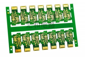
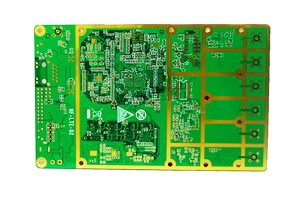
China Wholesale Speaker Pcb Board Quotes - 6 Layer High TG Leadless Golden Finger PCB – Huihe
When need high temperature PCBs? If the working temperature of the product is higher than 130 ℃, a high Tg PCB is required to ensure safety. The main reason for using high Tg PCB is that the PCB needs to comply with RoHS directive, and the temperature required for lead-free solder flow is high, resulting in the substrate of printed circuit board needs to be high Tg material. Application of the High Tg PCB TG PCB is used in electronic industry which can run at higher temperature. By ... -
China Wholesale Pcb Prototype Services Quotes - 8 Layer ENIG via-in-pad PCB – Huihe
The most difficult thing to control the plug hole in the via-in-pad is the solder ball or pad on the ink in the hole. Due to the necessity of using high density BGA (ball grid array) and the miniaturization of SMD chip, the application of in tray hole technology is more and more. Through the reliable through hole filling process, the in plate hole technology can be applied to the design and manufacture of high-density multilayer board, and avoid abnormal welding. Huihe Circuits has been using... -
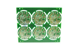
China Wholesale Pcb Tg Factories - 6 Layer ENIG via-in-pad PCB 16842 – Huihe
The advantages and disadvantages of plugging and no plugging? In terms of plug holes, they have the following advantages 1. the plug hole can prevent PCB through the wave soldering tin from the through hole through the component surface caused by short circuit; That is to say, within the scope of the wave soldering design area (generally the welding surface is 5mm or above) there is no hole or hole to do plug hole treatment. 2. The plug hole protects against possible short circuits caused by ... -
China Wholesale Populated Printed Circuit Boards Manufacturers - 6 Layer ENIG via-in-pad PCB 16842 – Huihe
The advantages and disadvantages of plugging and no plugging? In terms of plug holes, they have the following advantages 1. the plug hole can prevent PCB through the wave soldering tin from the through hole through the component surface caused by short circuit; That is to say, within the scope of the wave soldering design area (generally the welding surface is 5mm or above) there is no hole or hole to do plug hole treatment. 2. The plug hole protects against possible short circuits caused by ... -
China Wholesale Non Printed Circuit Board Manufacturers - 6 Layer High TG Leadless Golden Finger PCB – Huihe
When need high temperature PCBs? If the working temperature of the product is higher than 130 ℃, a high Tg PCB is required to ensure safety. The main reason for using high Tg PCB is that the PCB needs to comply with RoHS directive, and the temperature required for lead-free solder flow is high, resulting in the substrate of printed circuit board needs to be high Tg material. Application of the High Tg PCB TG PCB is used in electronic industry which can run at higher temperature. By ... -
China Wholesale Pcb Fabrication Manufacturers - 8 layer HASL PCB circuit board – Huihe
Why are multilayer boards mostly even? Due to the lack of a layer of medium and foil, the cost of raw materials for odd PCB is slightly lower than that for even PCB. However, the processing cost of odd layer PCB is significantly higher than that of even layer PCB. The processing cost of the inner layer is the same, but the foil/core structure significantly increases the processing cost of the outer layer. Odd layer PCB needs to add non-standard lamination core layer bonding process on th... -

China Wholesale Pcb Components Assembly Pricelist - 8 Layer ENIG Blind Buried Via PCB 12 – Huihe
About Level 1 Level 1 HDI technology refers to the laser blind hole only connected to the surface layer and its adjacent secondary layer hole forming technology. pressing in one time after drilling →utside again pressing copper foil → and then laser drilling About Level 1 Level 2 HDI PCB The Level 2 HDI technology is an improvement on the Level 1 HDI technology. It includes two forms of laser blind via drilling directly from the surface layer to the third layer, and laser blind... -

China Wholesale Flex Printed Circuit Board Manufacturers - 8 layer ENIG Impedance Control Heavy Copper PCB 16555 – Huihe
Thin core heavy copper PCB copper foil choice The most concerned problem of heavy copper CCL PCB is the pressure resistance problem, especially the thin core heavy copper PCB (thin core is medium thickness ≤ 0.3mm), the pressure resistance problem is particularly prominent, thin core heavy copper PCB will generally choose RTF copper foil for production, RTF copper foil and STD copper foil main difference is the length of the wool Ra is different, RTF copper foil Ra is significantly less ... -
China Wholesale Ssd Pcb Quotes - 8 Layer ENIG Impedance Control PCB – Huihe
Impedance is the combination of capacitance and inductance to hinder the circuit under high frequency signal. Impedance is an AC characteristic, which means it is frequency dependent. In the case of transmitting high-frequency signals, the controlled impedance helps to ensure that there is no significant attenuation of the signal during transmission. In essence, the controlled impedance means that the material characteristics of the substrate match the characteristics of the line / dielectric... -
China Wholesale High Quality Pcb Suppliers - 4 Layer FR4+Rogers PCB 29166 – Huihe
About High-frequency mixed-voltage PCB High-frequency mixed-voltage circuit boards are pressed using different laminated materials to optimize electrical performance and improve system reliability. The biggest challenge in manufacturing this type of high frequency PCB is to match the thermal expansion coefficient (CTE) of the different materials to fit the PCB manufacturing and component assembly. Typically, such circuit designs include a combination of FR-4 materials and PTFE laminated ... -
China Wholesale Round Pcb Manufacturers - 8 Layer ENIG Blind Buried Via PCB 12 – Huihe
About Level 1 Level 1 HDI technology refers to the laser blind hole only connected to the surface layer and its adjacent secondary layer hole forming technology. pressing in one time after drilling →utside again pressing copper foil → and then laser drilling About Level 1 Level 2 HDI PCB The Level 2 HDI technology is an improvement on the Level 1 HDI technology. It includes two forms of laser blind via drilling directly from the surface layer to the third layer, and laser blind... -
China Wholesale Pcb Order Suppliers - 8 Layer ENIG Blind Buried Via PCB 12 – Huihe
About Level 1 Level 1 HDI technology refers to the laser blind hole only connected to the surface layer and its adjacent secondary layer hole forming technology. pressing in one time after drilling →utside again pressing copper foil → and then laser drilling About Level 1 Level 2 HDI PCB The Level 2 HDI technology is an improvement on the Level 1 HDI technology. It includes two forms of laser blind via drilling directly from the surface layer to the third layer, and laser blind...


