-
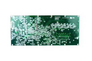
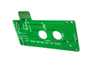
China Wholesale Understanding Circuit Boards Factories - 12 layer impedance Control HASL PCB – Huihe
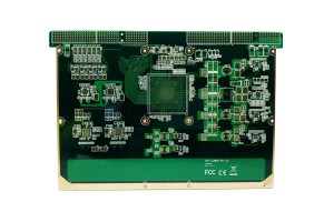
Why choose us? 1.Precision technology: it can process all kinds of high precision and high difficulty PCB, with 28 layers and 3 / 3mil line spacing 2.Professional Customization: to undertake proofing, batch PCB order demand 3.Advanced equipment: automatic copper deposition / electroplating line, LDI / CCD exposure machine and other equipment to produce high quality and high reliability products Our advantage As a professional PCB manufacturer, Huihe Circuits Co., Ltd. focuses on th... -

China Wholesale Rohs Pcb Pricelist - 6 Layer ENIG via-in-pad PCB 28203 – Huihe
Function of plug hole: The plug hole program of printed circuit board (PCB) is a process produced by the higher requirements of PCB manufacturing process and surface mount technology: 1.Avoid short circuit caused by tin penetrating through the component surface from the through hole during PCB over wave soldering 2.Avoid flux remaining in the through hole 3.Prevent solder bead from popping out during over wave soldering, resulting in short circuit 4.Prevent the surface solder paste from flow... -
China Wholesale Multisim Pcb Manufacturers - 6 Layer ENIG Blind Vias PCB 27809 – Huihe
Features of the Blind Via Blind Vias are located on the top and bottom surfaces of the circuit board and have a certain depth for the connection between the surface circuit and the inner circuit below. The depth of the hole usually does not exceed a certain ratio (aperture). This way of production will need to pay special attention to the depth of the hole (the Z axis) to the right, do not pay attention to words will cause difficult hole plating so almost no factory used, can also be connecte... -
China Wholesale Pcb Manufacturers - 4 Layer ENIG Blind Buried Via PCB – Huihe
About the HDI Due to the influence of drilling tool, the cost of traditional PCB drilling is very high when the drilling diameter reaches 0.15mm, and it is difficult to improve again. The drilling of HDI board no longer depends on the traditional mechanical drilling, but uses laser drilling technology. (so it is sometimes called laser plate.) The drilling hole diameter of HDI board is generally 3-5mil (0.076-0.127mm), and the line width is generally 3-4mil (0.076-0.10mm). The size of pad... -
China Wholesale Screen Printing Circuit Boards Factories - 6-layer ENIG impedance control PCB 15749 – Huihe
Differences between multilayer PCB and single panel / double-sided PC The biggest difference between multilayer PCB and single panel and double panel is that the internal power supply layer (to maintain the internal power layer) and the ground layer are added. The power supply and ground wire network are mainly wired on the power supply layer. However, the multilayer wiring is mainly the top and bottom layer, with the middle wiring layer as a supplement. Therefore, the design method of m... -
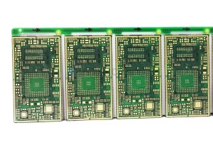
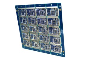
China Wholesale Embedded Pcb Pricelist - 8 Layer ENIG Impedance Control PCB 16978 – Huihe
Deficiencies of the blind buried vias The main problem of blind buried via is the high cost. In contrast, buried holes cost less than blind holes, but the use of both types of holes can significantly increase the cost of a board. The cost increase is due to the more complex manufacturing process of the blind buried hole, that is, the increase in manufacturing processes also leads to the increase in testing and inspection processes. Buried Via Buried vias are used to connect differen... -
China Wholesale High Current Pcb Manufacturers - 14 Layer Blind Buried Via PCB – Huihe
About Blind Buried Via PCB Blind vias and buried vias are two ways to establish connections between layers of printed circuit board. The blind vias of the printed circuit board are copper-plated vias that can be connected to the outer layer through most of the inner layer. The burrow connects two or more inner layers but does not penetrate the outer layer. Use microblind vias to increase line distribution density, improve radio frequency and electromagnetic interference, heat conduction,... -
China Wholesale Flex Printed Circuit Manufacturers - 6 Layer High TG Leadless Golden Finger PCB – Huihe
When need high temperature PCBs? If the working temperature of the product is higher than 130 ℃, a high Tg PCB is required to ensure safety. The main reason for using high Tg PCB is that the PCB needs to comply with RoHS directive, and the temperature required for lead-free solder flow is high, resulting in the substrate of printed circuit board needs to be high Tg material. Application of the High Tg PCB TG PCB is used in electronic industry which can run at higher temperature. By ... -
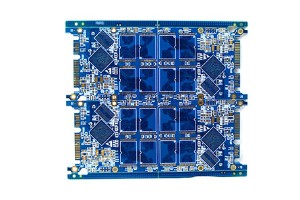
China Wholesale Printed Wiring Board Assembly Suppliers - 6 layer ENIG Heavy Copper PCB 15202 – Huihe
Crack problem of inner thick brazing pad The demand for heavy copper PCB is increasing, and the inner layer pads are getting smaller and smaller. The problem of pad cracking often occurs during PCB drilling (mainly for large holes above 2.5mm). There is little room for improvement in the material aspect of this kind of problem. The traditional improvement method is to increase the pad, increase the peeling strength of the material, and reduce the drilling rate, etc. Based on the analysis... -
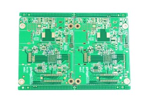
China Wholesale Surface Mount Prototype Board Pricelist - 10 layer ENIG impedance control PCB – Huihe
About Multilayer PCB Multilayer PCB refers to the multilayer PCB used in electrical products, multilayer board using more single or double panel wiring board. With a double lining, two one-way for outer layer or two double lining, two blocks of single outer layer of the printed circuit board, through the positioning and alternate insulation adhesive materials and conductive graphics interconnection according to design requirement of printed circuit board becomes four, six layer PCB, also... -
China Wholesale Hdi Pcb Manufacturers - 8 Layer ENIG Impedance Control PCB 16978 – Huihe
Deficiencies of the blind buried vias The main problem of blind buried via is the high cost. In contrast, buried holes cost less than blind holes, but the use of both types of holes can significantly increase the cost of a board. The cost increase is due to the more complex manufacturing process of the blind buried hole, that is, the increase in manufacturing processes also leads to the increase in testing and inspection processes. Buried Via Buried vias are used to connect differen... -
China Wholesale Circuit Board Components Suppliers - 4 Layer ENIG PCB 8329 – Huihe
Manufacturing technology of metallized half hole PCB The metallized half hole is cut in half after the round hole is formed. It is easy to appear the phenomenon of copper wire residue and copper leather warping in the half hole, which affects the function of the half hole and leads to the decrease of product performance and yield. In order to overcome the above defects, it shall be carried out according to the following process steps of metallized semi-orifice PCB 1. Processing half hole...


