-

China Wholesale Sensor Circuit Board Quotes - 6 Layer Rogers+ FR4 PCB – Huihe
The electrical, thermal and mechanical properties of high-frequency materials are different from those of conventional FR-4 materials. High frequency PCB has low dielectric constant Dk, low transmission delay, low loss factor Df and low dielectric loss. The high-frequency microwave board and RF board produced by Huihe Circuit include 5G base station antenna circuit board, 4G intermodulation antenna circuit board, high-precision impedance circuit board, high-frequency high-speed mixed voltage ... -
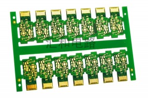
China Wholesale Production Of Pcb Manufacturers - 6 Layer ENIG via-in-pad PCB 16942 – Huihe
How to understand half plug hole and full plug hole The whole plug hole is the whole through hole is blocked by green oil. Generally, TOP and BOT fill the hole with green oil on both sides, and the fullness is more than 80%. The half plug hole refers to the plug from one side, opaque, half plug hole, fullness is not good control, general factory can only do about 30-50%, according to the factory’s own ability, mainly used in, one side of the window, one side of the window area, such as s... -
China Wholesale Printed Circuit Board Assembly Quotes - 6 Layer ENIG Blind Vias PCB 27809 – Huihe
Features of the Blind Via Blind Vias are located on the top and bottom surfaces of the circuit board and have a certain depth for the connection between the surface circuit and the inner circuit below. The depth of the hole usually does not exceed a certain ratio (aperture). This way of production will need to pay special attention to the depth of the hole (the Z axis) to the right, do not pay attention to words will cause difficult hole plating so almost no factory used, can also be connecte... -
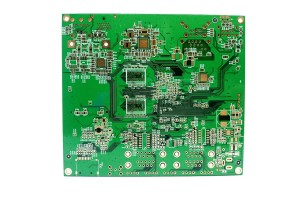
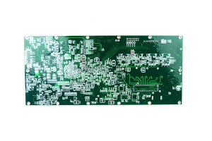
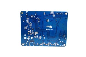
China Wholesale Load Board Pcb Quotes - 6 Layer ENIG Impedance Control PCB 7201 – Huihe
PCB impedance line design 1.In the process of PCB LAYOUT, consider the basic conditions required to control the impedance are: line width, line distance, line length, impedance line shielding reference layer, according to these requirements will be placed in the appropriate position of the impedance line. 2. The shielding reference layer preferentially selects the line adjacent to the layer where the impedance line is located. The corresponding position of the impedance line is a complete cop... -
China Wholesale Multisim Pcb Pricelist - 2 layer High TG ENIG PCB 11590 – Huihe
About High Tg material Tg is the mechanical property that specifies the glass transition temperature, the maximum temperature at which the glass remains rigid.Normal PCB FR4-TG is 130-140 degrees, medium TG is greater than 150-160 degrees, high TG is greater than 170 degrees. Compared with standard FR4, high FR4-TG has better mechanical and chemical heat resistance and moisture resistance.The higher the Tg value, the better the heat resistance of the material, so, especially in the lead-... -
China Wholesale Pcb Fabrication Manufacturers - 4 layer Taconic ENIG PCB 53 – Huihe
About PTFE PCB PTFE (commonly known as Teflon) is an ideal dielectric for RF applications, but it is not easily compatible with the conventional dielectric FR4 in PCB manufacturing. Ceramic dielectric is the most commonly used dielectric material in multilayer PCB. It can be used as a separate dielectric layer in special applications and as an inner dielectric layer in FR4 laminated structure in conventional applications. Many RF signal layers of RF design have large non copper filled ar... -

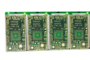
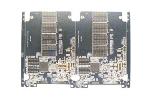
China Wholesale Printed Circuit Fabrication Quotes - 8 Layer ENIG Blind Buried Via PCB 12 – Huihe
About Level 1 Level 1 HDI technology refers to the laser blind hole only connected to the surface layer and its adjacent secondary layer hole forming technology. pressing in one time after drilling →utside again pressing copper foil → and then laser drilling About Level 1 Level 2 HDI PCB The Level 2 HDI technology is an improvement on the Level 1 HDI technology. It includes two forms of laser blind via drilling directly from the surface layer to the third layer, and laser blind... -
China Wholesale Load Board Pcb Pricelist - 6 Layer High TG Leadless Golden Finger PCB – Huihe
When need high temperature PCBs? If the working temperature of the product is higher than 130 ℃, a high Tg PCB is required to ensure safety. The main reason for using high Tg PCB is that the PCB needs to comply with RoHS directive, and the temperature required for lead-free solder flow is high, resulting in the substrate of printed circuit board needs to be high Tg material. Application of the High Tg PCB TG PCB is used in electronic industry which can run at higher temperature. By ... -
China Wholesale Rohs Circuit Board Manufacturers - 12 layer impedance Control HASL PCB – Huihe
Why choose us? 1.Precision technology: it can process all kinds of high precision and high difficulty PCB, with 28 layers and 3 / 3mil line spacing 2.Professional Customization: to undertake proofing, batch PCB order demand 3.Advanced equipment: automatic copper deposition / electroplating line, LDI / CCD exposure machine and other equipment to produce high quality and high reliability products Our advantage As a professional PCB manufacturer, Huihe Circuits Co., Ltd. focuses on th... -
China Wholesale Smt Circuit Boards Quotes - 4 Layer FR4+Rogers PCB 28848 – Huihe
The difficulty of laminated structure of mixed press PCB One of the major challenges in RF/microwave applications is how to ensure that the actual tolerances are within the design tolerances, so as to achieve the desired operating frequency. One of the biggest challenges in the lamination design of mixed-pressure structures is to have uniform thickness between different panels or even between different pieces. Due to the existence of a variety of substrate material types, there are a variety ... -
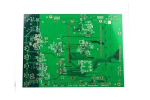
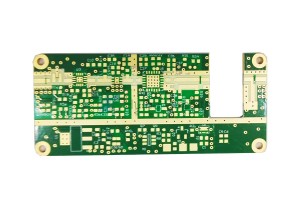
China Wholesale Pcb Clad Board Manufacturers - 6 Layer ENIG Impedance Control PCB 8931 – Huihe
Impedance characteristics of PCB According to the signal transmission theory, the signal is a function of time and distance variables, so every part of the signal on the line may change. Therefore, the AC impedance of the transmission line, that is, the ratio of voltage change to current change, is determined as the characteristic impedance of the transmission line. The characteristic impedance of the transmission line is only related to the characteristics of the signal connection itsel... -
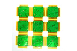
China Wholesale Castellated Pcb Pricelist - 6 Layer HASL Blind Buried Via PCB 13699 – Huihe
Features of the Buried Via The manufacturing process cannot be achieved by drilling after bonding. Drilling must be performed at individual circuit layers. The inner layer must be partially bonded first, followed by electroplating treatment, and then all bonded finally. This process is usually used only on high-density PCBs to increase the available space for other circuit layers The basic process of making HDI blind buried Via PCB Equipment display Automatic Plating Lin...


