-
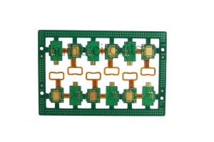
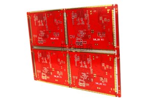
China Wholesale Pcb Clad Board Suppliers - 4 Layer FPC+FR4 Rigid Flex PCB 20 – Huihe
Design rules and precautions of Rigid Flex PCB The design of rigid flex PCB is much more complex than the traditional PCB design, and there are many places to pay attention to. In particular, the rigid flexible transition area, as well as the related wiring, through-hole design, all need to follow the requirements of the corresponding design rules. 1. Through hole position In the case of dynamic use, especially when the soft plate is often bent, the through holes on the soft plate should... -
China Wholesale Electronic Circuit Board Assembly Suppliers - 6 Layer High TG Leadless Golden Finger PCB – Huihe
When need high temperature PCBs? If the working temperature of the product is higher than 130 ℃, a high Tg PCB is required to ensure safety. The main reason for using high Tg PCB is that the PCB needs to comply with RoHS directive, and the temperature required for lead-free solder flow is high, resulting in the substrate of printed circuit board needs to be high Tg material. Application of the High Tg PCB TG PCB is used in electronic industry which can run at higher temperature. By ... -
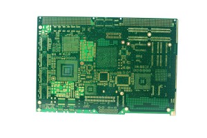
China Wholesale Pcb Board Components Factories - 16 Layer ENIG Press Fit Hole PCB 31525 – Huihe
About Via-In-Pad PCB The Via-In-Pad PCBs are generally blind holes, which are mainly used to connect the inner layer or the secondary outer layer of HDI PCB with the outer layer, so as to improve the electrical performance and reliability of electronic products, shorten the signal transmission wire, reduce the inductive reactance and capacitive reactance of the transmission line, as well as the internal and external electromagnetic interference. It’s used for conducting. The main problem... -
China Wholesale Pcb Pwb Suppliers - 4 Layer FPC+FR4 Rigid Flex PCB 20 – Huihe
Design rules and precautions of Rigid Flex PCB The design of rigid flex PCB is much more complex than the traditional PCB design, and there are many places to pay attention to. In particular, the rigid flexible transition area, as well as the related wiring, through-hole design, all need to follow the requirements of the corresponding design rules. 1. Through hole position In the case of dynamic use, especially when the soft plate is often bent, the through holes on the soft plate should... -
China Wholesale Complex Circuit Board Suppliers - 10 Layer ENIG Blind Vias PCB 28526 – Huihe
About Blind Buried Via PCB Blind Via: which enables the connection and conduction between the inner and outer layers Buried Via: which can connect and guide between inner layers Blind Vias are mostly small holes with a diameter of 0.05mm~0.15mm. There are laser hole forming, plasma etched hole and photoinduced hole forming, and laser hole forming is usually used. HDI: High-density interconnection, non-mechanical drilling, micro-blind hole ring below 6mil, inside and outside layers of wiring l... -
China Wholesale Elevator Circuit Boards Quotes - 8 Layer impedance ENIG PCB 6351 – Huihe
Half hole technology After the PCB is made in the half hole, the tin layer is set at the edge of the hole by electroplating. The tin layer is used as the protective layer to enhance the tear resistance and completely prevent the copper layer falling off from the hole wall. Therefore, the impurity generation in the production process of the printed circuit board is reduced, and the workload of cleaning is also reduced, so as to improve the quality of the finished PCB. After the production... -
China Wholesale Double Sided Pcb Factories - 14 Layer Blind Buried Via PCB – Huihe
About Blind Buried Via PCB Blind vias and buried vias are two ways to establish connections between layers of printed circuit board. The blind vias of the printed circuit board are copper-plated vias that can be connected to the outer layer through most of the inner layer. The burrow connects two or more inner layers but does not penetrate the outer layer. Use microblind vias to increase line distribution density, improve radio frequency and electromagnetic interference, heat conduction,... -
China Wholesale Smt Boards Quotes - 6 Layer ENIG Blind Vias PCB 27809 – Huihe
Features of the Blind Via Blind Vias are located on the top and bottom surfaces of the circuit board and have a certain depth for the connection between the surface circuit and the inner circuit below. The depth of the hole usually does not exceed a certain ratio (aperture). This way of production will need to pay special attention to the depth of the hole (the Z axis) to the right, do not pay attention to words will cause difficult hole plating so almost no factory used, can also be connecte... -
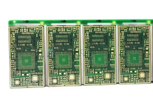
China Wholesale Pcb Service Factories - 8 Layer ENIG via-in-pad PCB – Huihe
The most difficult thing to control the plug hole in the via-in-pad is the solder ball or pad on the ink in the hole. Due to the necessity of using high density BGA (ball grid array) and the miniaturization of SMD chip, the application of in tray hole technology is more and more. Through the reliable through hole filling process, the in plate hole technology can be applied to the design and manufacture of high-density multilayer board, and avoid abnormal welding. Huihe Circuits has been using... -

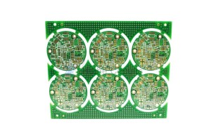
China Wholesale Round Pcb Manufacturers - 6 layer ENIG Impedance Control Heavy Copper PCB 15881 – Huihe
Functions of heavy copper PCB Heavy copper PCB has the best extension functions, is not limited by the processing temperature, high melting point can be used oxygen blowing, low temperature at the same brittle and other hot melt welding, but also fire prevention, belongs to the non-combustible material. Even in highly corrosive atmospheric conditions, copper sheets form a strong, non-toxic passivation protective layer. Difficulty in machining control of heavy copper PCB Thickness of copper PC... -
China Wholesale Power Supply Pcb Board Factories - 6 layer ENIG impedance control PCB 16403 – Huihe
About Multilayer PCB With the increasing complexity of circuit design, in order to increase the area of wiring, multilayer PCB can be used. Multilayer board is a PCB that contains multiple working layers. In addition to the top and bottom layers, it also includes signal layer, middle layer, internal power supply and ground layer. The number of layers of PCB represents that there are several independent wiring layers. Generally, the number of layers is even and includes the outermost two ... -
China Wholesale Understanding Circuit Boards Factories - 12 Layer ENIG PCB 14799 – Huihe
HDI PCB material HDI PCB materials are RCC, LDPE, FR4 RCC:Resin coated Copper is short for resin coated copper foil. RCC is composed of copper foil and resin with rough surface, heat resistance and anti-oxidation treatment (used when the thickness is more than 4mil) The resin layer of RCC has the same processability as FR4 adhesive sheet (prepreg). In addition, it should also meet the relevant performance requirements of the laminate, such as: At the same time, because RCC is a new type ...


