-
China Wholesale Fast Turn Pcb Factories - 6 Layer ENIG Impedance Control PCB 7201 – Huihe
PCB impedance line design 1.In the process of PCB LAYOUT, consider the basic conditions required to control the impedance are: line width, line distance, line length, impedance line shielding reference layer, according to these requirements will be placed in the appropriate position of the impedance line. 2. The shielding reference layer preferentially selects the line adjacent to the layer where the impedance line is located. The corresponding position of the impedance line is a complete cop... -
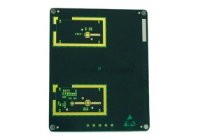
China Wholesale Transparent Circuit Board Manufacturers - 4 Layer Rogers PCB 29671 – Huihe
About High frequency PCB High frequency PCB refers to the special circuit board with high electromagnetic frequency, which is used for high frequency (frequency greater than 300MHz or wavelength in general, high frequency board can be defined as the circuit board with frequency above 1GHz. Substrate materials need to have excellent electrical properties, good chemical stability, with the increase of power signal frequency in the substrate loss requirements are very small. Difficulties... -

China Wholesale Flexible Pcb Prototype Quotes - 8 Layer ENIG Blind Buried Via PCB 12 – Huihe
About Level 1 Level 1 HDI technology refers to the laser blind hole only connected to the surface layer and its adjacent secondary layer hole forming technology. pressing in one time after drilling →utside again pressing copper foil → and then laser drilling About Level 1 Level 2 HDI PCB The Level 2 HDI technology is an improvement on the Level 1 HDI technology. It includes two forms of laser blind via drilling directly from the surface layer to the third layer, and laser blind... -
China Wholesale Pcb Prototype Services Quotes - 8 Layer FPC+FR4 Rigid Flex PCB 4 – Huihe
The Rigid Flex PCB plays a key role in the automotive market The Rigid Flex PCB is becoming more and more important in automotive electronics, which is beyond PCB operators’ original imagination. The reason is that we did not think that the technology used in mobile phone lens module would have the opportunity to extend to the ADAS lens module for car, and further attract the auto component industry to introduce the Rigid Flex PCB into the module products such as photar, and become the entry ... -
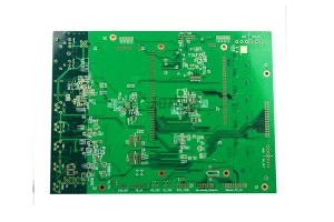
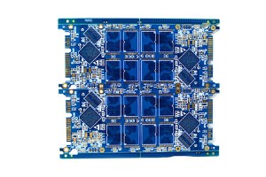
China Wholesale Pcb Pwb Quotes - 6 layer ENIG impedance control PCB 16403 – Huihe
About Multilayer PCB With the increasing complexity of circuit design, in order to increase the area of wiring, multilayer PCB can be used. Multilayer board is a PCB that contains multiple working layers. In addition to the top and bottom layers, it also includes signal layer, middle layer, internal power supply and ground layer. The number of layers of PCB represents that there are several independent wiring layers. Generally, the number of layers is even and includes the outermost two ... -
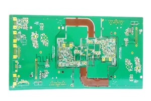
China Wholesale Mosfet Pcb Manufacturers - 2 Layer High TG Heavy Copper PCB 11 – Huihe
About the heavy copper PCB Heavy copper PCB has the characteristics of carrying large current, reducing thermal strain and good heat dissipation. Increasing copper thickness has become an effective way for many terminal design manufacturers to seek solutions. There are more and more heavy copper PCB products, as a special product in product design, CCL production and PCB processing, there are many production difficulties and matters needing attention and solution. CCL is the raw material... -
China Wholesale Prototype Pcb Board Pricelist - 4 layer ENIG Impedance Control Heavy Copper PCB 15059 – Huihe
Precautions for engineering design of heavy copper PCB With the development of electronic technology, the volume of PCB is more and more small, density is becoming more and more high, and the PCB layers increasing, therefore, requires PCB on integral layout, anti-interference ability, process and manufacturability demand is higher and higher, as the content of engineering design very much, mainly for heavy copper PCB manufacturability, craft workability and the reliability of the product... -
China Wholesale Pcb Speaker Suppliers - 8 Layer ENIG Blind Buried Via PCB 12 – Huihe
About Level 1 Level 1 HDI technology refers to the laser blind hole only connected to the surface layer and its adjacent secondary layer hole forming technology. pressing in one time after drilling →utside again pressing copper foil → and then laser drilling About Level 1 Level 2 HDI PCB The Level 2 HDI technology is an improvement on the Level 1 HDI technology. It includes two forms of laser blind via drilling directly from the surface layer to the third layer, and laser blind... -
China Wholesale Circuit Board Components Quotes - 4 layer Medium TG ENIG PCB 13270 – Huihe
About High Tg PCB High Tg means high heat resistance. With the rapid development of the electronic industry, especially the electronic products represented by computers, the development of high functionalization and high multilayer requires the higher heat resistance of PCB substrate materials as an important guarantee. With the emergence and development of high density installation technology, such as SMT and CMT, PCB is increasingly dependent on the support of high heat resistance of t... -
China Wholesale Nixie Clock Pcb Suppliers - 8 layer HASL PCB circuit board – Huihe
Why are multilayer boards mostly even? Due to the lack of a layer of medium and foil, the cost of raw materials for odd PCB is slightly lower than that for even PCB. However, the processing cost of odd layer PCB is significantly higher than that of even layer PCB. The processing cost of the inner layer is the same, but the foil/core structure significantly increases the processing cost of the outer layer. Odd layer PCB needs to add non-standard lamination core layer bonding process on th... -
China Wholesale Flex Pcbs Quotes - 6-layer ENIG impedance control PCB 15749 – Huihe
Differences between multilayer PCB and single panel / double-sided PC The biggest difference between multilayer PCB and single panel and double panel is that the internal power supply layer (to maintain the internal power layer) and the ground layer are added. The power supply and ground wire network are mainly wired on the power supply layer. However, the multilayer wiring is mainly the top and bottom layer, with the middle wiring layer as a supplement. Therefore, the design method of m... -
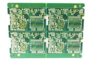
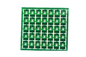
China Wholesale Ic Circuit Board Suppliers - 10 Layer ENIG Blind Vias PCB 28526 – Huihe
About Blind Buried Via PCB Blind Via: which enables the connection and conduction between the inner and outer layers Buried Via: which can connect and guide between inner layers Blind Vias are mostly small holes with a diameter of 0.05mm~0.15mm. There are laser hole forming, plasma etched hole and photoinduced hole forming, and laser hole forming is usually used. HDI: High-density interconnection, non-mechanical drilling, micro-blind hole ring below 6mil, inside and outside layers of wiring l...


