-
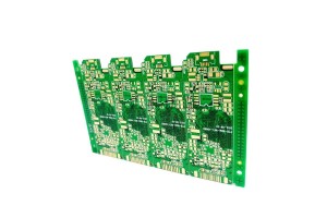
China Wholesale Populated Printed Circuit Boards Factories - 6 Layer ENIG Impedance Control PCB 14706 – Huihe
Difference between pad and via 1. Definitions differ Pad: is the basic unit of surface mount assembly, which is used to form the landpattern of the circuit board, that is, a variety of combinations of pads designed for special component types. Through hole: through hole is also called metallization hole. In the double panel and multilayer PCB, a common hole is drilled at the junction of the wires that need to be connected between the layers in order to connect the printed wires between l... -
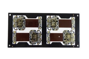
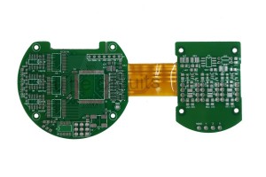
China Wholesale Flex Printed Circuit Board Factories - 6 Layer FPC+FR4 Rigid-Flex PCB 9 – Huihe
About the Rigid-Flex PCB Rigid-flex PCB is a new type of PCB with both the durability of rigid pcb and the adaptability of flexible PCB. In all types of PCB, the rigid-flex PCB is the most resistant to harsh application environment. Therefore, it is favored by industrial control, medical and military equipment manufacturers. The rigid-flex PCB factories in the mainland are gradually increasing the proportion of flexible and rigid PCB in the total output. Advantages and disadvantages of Rigid-... -
China Wholesale Teflon Pcb Board Factories - 14 Layer High TG Fine Pitch PCB 14 – Huihe
About High Tg PCB The general TG is more than 130 degrees, the high Tg is more than 170 degrees, and the medium TG is more than 150 degrees. Generally, PCB with TG ≥ 170 ℃ is called high Tg PCB. When the Tg of the substrate is increased, the heat resistance, moisture resistance, chemical resistance, stability resistance and other characteristics of the circuit board will be improved. The higher the TG value, the better the temperature resistance of the sheet, especially in the lead-free ... -
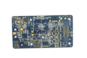
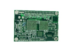
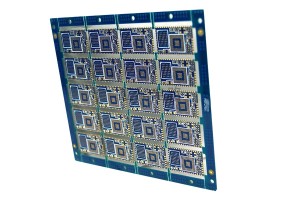
China Wholesale Prototype Pcb Board Manufacturers - 4 layer ENIG Impedance Control Heavy Copper PCB 15059 – Huihe
Precautions for engineering design of heavy copper PCB With the development of electronic technology, the volume of PCB is more and more small, density is becoming more and more high, and the PCB layers increasing, therefore, requires PCB on integral layout, anti-interference ability, process and manufacturability demand is higher and higher, as the content of engineering design very much, mainly for heavy copper PCB manufacturability, craft workability and the reliability of the product... -
China Wholesale Hitech Pcb Manufacturers - 2 layer ENIG Heavy Copper PCB 15872 – Huihe
Difficulties in drilling heavy copper PCBs With the increase of the copper thickness, the thickness of the heavy copper PCB also increases. heavy copper PCB is usually more than 2.0mm thick, drilling production due to the thickness of the thickness of the plate and copper thick factors, production is more difficult. In this regard, the use of a new cutter, reduce the service life of the drill cutter, section drilling has become an effective solution to the heavy copper PCB drilling. In a... -
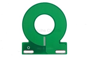
China Wholesale Flexible Pcb Factories - 2 Layer High TG Heavy Copper PCB 11 – Huihe
About the heavy copper PCB Heavy copper PCB has the characteristics of carrying large current, reducing thermal strain and good heat dissipation. Increasing copper thickness has become an effective way for many terminal design manufacturers to seek solutions. There are more and more heavy copper PCB products, as a special product in product design, CCL production and PCB processing, there are many production difficulties and matters needing attention and solution. CCL is the raw material... -
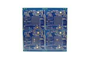
China Wholesale Prototype Pcb Assembly Factories - 8 Layer impedance ENIG PCB 6351 – Huihe
Half hole technology After the PCB is made in the half hole, the tin layer is set at the edge of the hole by electroplating. The tin layer is used as the protective layer to enhance the tear resistance and completely prevent the copper layer falling off from the hole wall. Therefore, the impurity generation in the production process of the printed circuit board is reduced, and the workload of cleaning is also reduced, so as to improve the quality of the finished PCB. After the production... -
China Wholesale Motion Sensor Circuit Board Quotes - 6 Layer ENIG Impedance Control PCB 9806 – Huihe
About the impedance Impedance is the combination of capacitance and inductance to block the circuit in high frequency signal. Impedance is a kind of AC characteristic, which means that it is related to frequency and is used to describe the high frequency characteristics of PCB. Factors affecting impedance DK (R): determined by raw materials (PCB material, semi cured sheet) Line thickness (T): determined by raw materials and process capability. Line width (W): determined by customer’... -
China Wholesale Rohs Circuit Board Manufacturers - 4 Layer ENIG PCB 8329 – Huihe
Manufacturing technology of metallized half hole PCB The metallized half hole is cut in half after the round hole is formed. It is easy to appear the phenomenon of copper wire residue and copper leather warping in the half hole, which affects the function of the half hole and leads to the decrease of product performance and yield. In order to overcome the above defects, it shall be carried out according to the following process steps of metallized semi-orifice PCB 1. Processing half hole... -

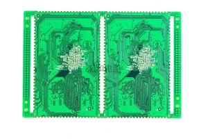
China Wholesale Rf Circuit Board Suppliers - 6 Layer ENIG Impedance Control PCB 10222 – Huihe
Factors determining controlled impedance The characteristic impedance of a PCB is usually determined by its inductance and capacitance, resistance and conductance. These factors are functions of the physical size of the circuit, the dielectric constant and dielectric thickness of the PCB substrate material. In general, the line impedance of a PCB ranges from 25 to 125Ω. The PCB structure that determines the impedance value consists of the following factors: Width and thickness of top and... -
China Wholesale Power Supply Pcb Board Quotes - 4 Layer SF302+FR4 Rigid-Flex PCB 19 – Huihe
Points for attention in the design of rigid flexible combination zone 1.The line should transition smoothly, and the direction of the line should be perpendicular to the bending direction. 2.The conductor shall be evenly distributed throughout the bending zone. 3.The width of the conductor shall be maximized throughout the bending zone. 4.PTH design should not be used in rigid flexible transition zone. 5.Bending radius of bending zone of rigid flexible PCB Material of flexible PCB E... -

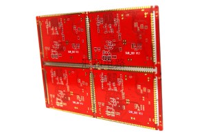
China Wholesale Rf Pcb Pricelist - 8 Layer ENIG Blind Buried Via PCB 12 – Huihe
About Level 1 Level 1 HDI technology refers to the laser blind hole only connected to the surface layer and its adjacent secondary layer hole forming technology. pressing in one time after drilling →utside again pressing copper foil → and then laser drilling About Level 1 Level 2 HDI PCB The Level 2 HDI technology is an improvement on the Level 1 HDI technology. It includes two forms of laser blind via drilling directly from the surface layer to the third layer, and laser blind...


