-
China Wholesale Automatic Stabilizer Circuit Board Manufacturers - 14 Layer Blind Buried Via PCB – Huihe
About Blind Buried Via PCB Blind vias and buried vias are two ways to establish connections between layers of printed circuit board. The blind vias of the printed circuit board are copper-plated vias that can be connected to the outer layer through most of the inner layer. The burrow connects two or more inner layers but does not penetrate the outer layer. Use microblind vias to increase line distribution density, improve radio frequency and electromagnetic interference, heat conduction,... -
China Wholesale Order Printed Circuit Board Quotes - 6 Layer FR4+Rogers PCB 28727 – Huihe
Features of high frequency PCB 1. High frequency PCB with small dielectric constant, loss will be very small, and advanced induction heating technology can achieve the needs of the target heating, very high efficiency. Of course, while paying attention to efficiency, it also has the characteristics of environmental protection, which is very suitable for the development direction of today’s society. 2. The transmission speed is inversely proportional to the square root of the dielec... -
China Wholesale Make Custom Pcb Pricelist - 2 Layer in spray half hole PCB 14146 – Huihe
About metallizing half-hole PCB Metal half hole (groove) is a hole after the hole after the second drilling, shape process, and finally retain the metal hole (groove) half, simply said that the plate edge metallized hole cut half, the plate edge semi-metallic hole process is a very mature process. How to control the product quality after forming the semi-metallic hole on the edge of the plate. Such as hole wall copper prickle, residual has been a difficult process. A full row of semi-met... -
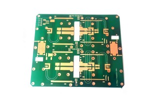
China Wholesale Panel Circuit Board Suppliers - 4 layer Taconic ENIG PCB 53 – Huihe
About PTFE PCB PTFE (commonly known as Teflon) is an ideal dielectric for RF applications, but it is not easily compatible with the conventional dielectric FR4 in PCB manufacturing. Ceramic dielectric is the most commonly used dielectric material in multilayer PCB. It can be used as a separate dielectric layer in special applications and as an inner dielectric layer in FR4 laminated structure in conventional applications. Many RF signal layers of RF design have large non copper filled ar... -
China Wholesale Non Printed Circuit Board Factories - 2 Layer in spray half hole PCB 14146 – Huihe
About metallizing half-hole PCB Metal half hole (groove) is a hole after the hole after the second drilling, shape process, and finally retain the metal hole (groove) half, simply said that the plate edge metallized hole cut half, the plate edge semi-metallic hole process is a very mature process. How to control the product quality after forming the semi-metallic hole on the edge of the plate. Such as hole wall copper prickle, residual has been a difficult process. A full row of semi-met... -
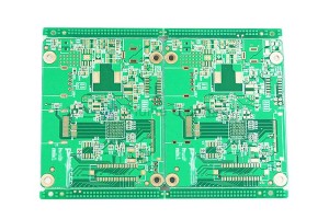
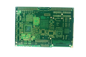
China Wholesale Red Circuit Board Suppliers - 4 Layer ENIG Blind Buried Via PCB – Huihe
About the HDI Due to the influence of drilling tool, the cost of traditional PCB drilling is very high when the drilling diameter reaches 0.15mm, and it is difficult to improve again. The drilling of HDI board no longer depends on the traditional mechanical drilling, but uses laser drilling technology. (so it is sometimes called laser plate.) The drilling hole diameter of HDI board is generally 3-5mil (0.076-0.127mm), and the line width is generally 3-4mil (0.076-0.10mm). The size of pad... -
China Wholesale Pcb Vendor Pricelist - 6 Layer ENIG Impedance Control PCB 14706 – Huihe
Difference between pad and via 1. Definitions differ Pad: is the basic unit of surface mount assembly, which is used to form the landpattern of the circuit board, that is, a variety of combinations of pads designed for special component types. Through hole: through hole is also called metallization hole. In the double panel and multilayer PCB, a common hole is drilled at the junction of the wires that need to be connected between the layers in order to connect the printed wires between l... -

China Wholesale Solder Circuit Board Pricelist - 6 layer High TG ENIG PCB 10845 – Huihe
Difference between general FR4 and high Tg FR4 The difference between general FR-4 and high FR4-TG lies in the difference of mechanical strength, adhesion, water absorption, dimensional stability, thermal decomposition of hot state (especially after water absorption) under hot state under different conditions (such as thermal expansion). Obviously, high Tg PCB is better than ordinary PCB substrate material. Therefore, in recent years, there is a great demand for high Tg PCB, but the pric... -
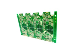
China Wholesale Euro Pcb Pricelist - 6 Layer HASL Blind Buried Via PCB 13699 – Huihe
Features of the Buried Via The manufacturing process cannot be achieved by drilling after bonding. Drilling must be performed at individual circuit layers. The inner layer must be partially bonded first, followed by electroplating treatment, and then all bonded finally. This process is usually used only on high-density PCBs to increase the available space for other circuit layers The basic process of making HDI blind buried Via PCB Equipment display Automatic Plating Lin... -
China Wholesale Pcba Factories - 4 Layer FR4+Rogers PCB 28848 – Huihe
The difficulty of laminated structure of mixed press PCB One of the major challenges in RF/microwave applications is how to ensure that the actual tolerances are within the design tolerances, so as to achieve the desired operating frequency. One of the biggest challenges in the lamination design of mixed-pressure structures is to have uniform thickness between different panels or even between different pieces. Due to the existence of a variety of substrate material types, there are a variety ... -
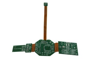
China Wholesale Timer Circuit Board Suppliers - 4 Layer FPC+FR4 Rigid-Flex PCB – Huihe
About the Rigid-Flex PCB Rigid-Flex PCB, is the flexible PCB and traditional Rigid PCB, after many procedures, according to the relevant process requirements combined together, forming at the same time with FPC characteristics and PCB characteristics of the circuit board. It can be used in some products with special requirements, both a certain flexible area and a certain rigid area, to save the internal space of the product, reduce the volume of finished products, improve the performance of ... -
China Wholesale Custom Made Pcb Boards Factories - 2 Layer High TG Heavy Copper PCB 11 – Huihe
About the heavy copper PCB Heavy copper PCB has the characteristics of carrying large current, reducing thermal strain and good heat dissipation. Increasing copper thickness has become an effective way for many terminal design manufacturers to seek solutions. There are more and more heavy copper PCB products, as a special product in product design, CCL production and PCB processing, there are many production difficulties and matters needing attention and solution. CCL is the raw material...


