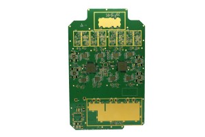
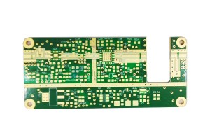
6 Layer ENIG FR4 Via-In-Pad PCB

Function Of Plug Hole
The plug hole program of printed circuit board (PCB) is a process produced by the higher requirements of PCB manufacturing process and surface mount technology:
1.Avoid short circuit caused by tin penetrating through the component surface from the through hole during PCB over wave soldering.
2.Avoid flux remaining in the through hole.
3.Prevent solder bead from popping out during over wave soldering, resulting in short circuit.
4.Prevent the surface solder paste from flowing into the hole, causing false soldering and affecting the mounting.
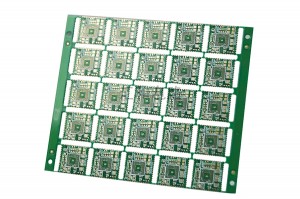
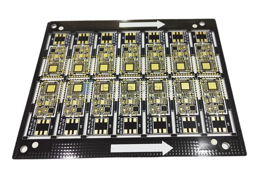
Via In pad Process
Ddefine
For the holes of some small parts to be welded on the ordinary PCB , the traditional production method is to drill a hole on the board, and then coat a layer of copper in the hole to realize the conduction between layers, and then lead a wire to connect a welding pad to complete the welding with the outside parts.
Development
The Via in Pad manufacturing process is being developed against the backdrop of increasingly dense, interconnected circuit boards, where there is no more room for the wires and pads that connect the through holes.
Fuction
The production process of VIA IN PAD makes the PCB production process three-dimensional, effectively saves the horizontal space, and ADAPTS to the development trend of modern circuit board with high density and interconnection.
Factory Show

PCB Manufacturing Base

Admin Receptionist

Meeting Room