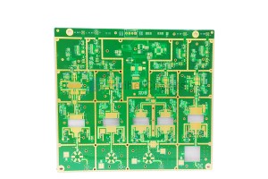
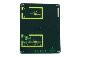
4 Layer ENIG FR4+R04350 Mixed Lamination PCB


FR4+Rogers Mixing Lamination PCB manufacturing Difficulties
One of the major challenges in RF/microwave applications is how to ensure that the actual tolerances are within the design tolerances, so as to achieve the desired operating frequency. One of the biggest challenges in the lamination design of mixed-pressure structures is to have uniform thickness between different panels or even between different pieces. Due to the existence of a variety of substrate material types, there are a variety of semi-cured sheet types.
Rogers is different from traditional PCB epoxy resin. There is no glass fiber in the middle and it is a ceramic based high frequency material. At circuit frequencies above 500MHz, the range of materials available to the design engineer is greatly reduced. Rogers RO4350B material can be easily made RF engineering design circuits, such as network matching, transmission line impedance control, etc. Due to its low dielectric loss, R04350B has an advantage over common circuit materials in high frequency applications. The dielectric constant of temperature fluctuation is almost the lowest in the same material. The permittivity is also remarkably stable at 3.48 over a wide frequency range. 3.66. Lopra copper foil design recommendations to reduce insertion loss. This makes the material suitable for broadband applications.
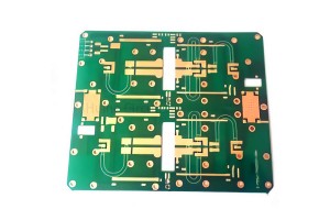
Advantages Of Mixing Lamination High Frequency PCB
1. High-frequency PCB has high density and improved signal. It offers a frequency range from 500MHz to 2GHz, ideal for high-speed designs.
2. The use of the ground layer further improves the signal quality and reduces the electromagnetic wave.
3.Reduce circuit impedance and provide shielding effect.
4. By reducing the distance between the plane and the routing layer, crosstalk can be avoided
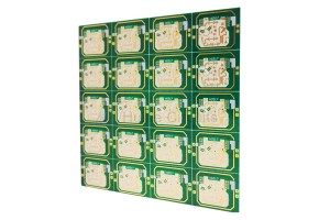
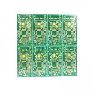
Factory Show

PCB Manufacturing Base

Admin Receptionist

Meeting Room