-
New Arrival China Custom Pcb China - 10 Layer ENIG FR4 Blind Vias PCB – Huihe
About Blind Buried Via PCB Blind Via: which enables the connection and conduction between the inner and outer layers Buried Via: which can connect and guide between inner layers Blind Vias are mostly small holes with a diameter of 0.05mm~0.15mm. There are laser hole forming, plasma etched hole and photoinduced hole forming, and laser hole forming is usually used. HDI: High-density interconnection, non-mechanical drilling, micro-blind hole ring below 6mil, inside and outside layers of wiring l... -
Factory wholesale Led Printed Circuit Board - 2 Layer HASL FR4 Half Hole PCB – Huihe
About Metallizing Half-Hole PCB Metal half hole (groove) is a hole after the hole after the second drilling, shape process, and finally retain the metal hole (groove) half, simply said that the plate edge metallized hole cut half, the plate edge semi-metallic hole process is a very mature process. How to control the product quality after forming the semi-metallic hole on the edge of the plate. Such as hole wall copper prickle, residual has been a difficult process. A full row of semi-metalliz... -

OEM/ODM China China Rigid Flex Pcb Factory - 6 Layer ENIG Impedance Control Heavy Copper PCB – Huihe
Functions Of Heavy Copper PCB Heavy copper PCB has the best extension functions, is not limited by the processing temperature, high melting point can be used oxygen blowing, low temperature at the same brittle and other hot melt welding, but also fire prevention, belongs to the non-combustible material. Even in highly corrosive atmospheric conditions, copper sheets form a strong, non-toxic passivation protective layer. Difficulty In Machining Control Of Heavy Copper PCB Thickness of copper PC... -
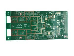
Factory Promotional Copper Base Pcb Quotes - 6 Layer FR4 ENIG Impedance Control PCB – Huihe
Difference Between Pad And Via 1. Definitions Differ Pad: is the basic unit of surface mount assembly, which is used to form the landpattern of the circuit board, that is, a variety of combinations of pads designed for special component types. Through hole: through hole is also called metallization hole. In the double panel and multilayer PCB, a common hole is drilled at the junction of the wires that need to be connected between the layers in order to connect the printed wires between layers... -
Factory selling Six-Layer Enig Impedance Half Hole Pcb - 2 Layer HASL FR4 Half Hole PCB – Huihe
About Metallizing Half-Hole PCB Metal half hole (groove) is a hole after the hole after the second drilling, shape process, and finally retain the metal hole (groove) half, simply said that the plate edge metallized hole cut half, the plate edge semi-metallic hole process is a very mature process. How to control the product quality after forming the semi-metallic hole on the edge of the plate. Such as hole wall copper prickle, residual has been a difficult process. A full row of semi-metalliz... -
Factory Supply Quick-Turn Pcb - 6 Layer ENIG FR4 Blind Vias PCB – Huihe
Features Of The Blind Via PCB Blind Vias are located on the top and bottom surfaces of the circuit board and have a certain depth for the connection between the surface circuit and the inner circuit below. The depth of the hole usually does not exceed a certain ratio (aperture). This way of production will need to pay special attention to the depth of the hole (the Z axis) to the right, do not pay attention to words will cause difficult hole plating so almost no factory used, can also be conn... -
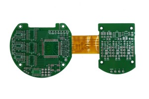
China Supplier Pcb Board Supplier In China - 4 Layer ENIG SF302+FR4 Rigid-Flex PCB – Huihe
Points For Attention In The Design Of Rigid Flexible Combination Zone 1.The line should transition smoothly, and the direction of the line should be perpendicular to the bending direction. 2.The conductor shall be evenly distributed throughout the bending zone. 3.The width of the conductor shall be maximized throughout the bending zone. 4.PTH design should not be used in rigid flexible transition zone. 5.Bending radius of bending zone of rigid flexible PCB Material Of Flexible PCB Everyone is... -
High reputation Pcb Components Assembly - 12 Layer HASL Multilayer FR4 PCB – Huihe
Why Choose HUIHE Circuits For Multilayer PCB? 1.Precision technology: it can process all kinds of high precision and high difficulty PCB, with 28 layers and 3/3mil line spacing 2.Professional Customization: PCB prototype, high volume PCB order demand 3.Advanced equipment: automatic copper deposition/electroplating line, LDI/CCD exposure machine and other equipment to produce high quality and high reliability products Our Advantages Of Making Multilayer PCB As a professional PCB man... -
High reputation Fr4 High Tg - 4 Layer ENIG FR4+RO4350 Mixed Lamination PCB – Huihe
Mixed Lamination High Frequency PCB Mixed lamination high frequency PCB circuit boards are pressed using different laminated materials to optimize electrical performance and improve system reliability. The biggest challenge in manufacturing this type of high frequency PCB is to match the thermal expansion coefficient (CTE) of the different materials to fit the PCB manufacturing and component assembly. Typically, such circuit designs include a combination of FR-4 materials and PTFE lamin... -
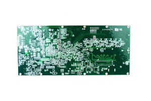
8 Year Exporter Printed Circuit Board China - 8 Layer ENIG FR4 Multilayer PCB – Huihe
The Difficulty Of Multilayer PCB Board Prototyping 1. The difficulty of interlayer alignment Because of the many layers of multilayer PCB board, the calibration requirement of PCB layer is higher and higher. Typically, alignment tolerance between layers is controlled at 75um. It is more difficult to control the alignment of multilayer PCB board because of the large size of the unit, the high temperature and humidity in the graphics conversion workshop, the dislocation overlap caused by t... -
China Gold Supplier for Multilayer Board Supplier - 12 Layer ENIG FR4+Rogers Mixed Lamination High Frequency PCB – Huihe
Mixed Lamination High Frequency PCB Board There are three main reasons for using mixed lamination high frequency PCBs: cost, improved reliability and enhanced electrical performance. 1. Hf line materials are much more expensive than FR4. Sometimes, using mixed lamination of FR4 and hf lines can solve the cost problem. 2. In many cases, some lines of mixed lamination high frequency PCB board require high electrical performance, and some do not. 3. FR4 is used for the less electrically d... -
Factory Cheap Rohs Pcb Board Manufacturer - 4 Layer ENIG FR4+RO4350 Mixed Lamination PCB – Huihe
Mixed Lamination High Frequency PCB Mixed lamination high frequency PCB circuit boards are pressed using different laminated materials to optimize electrical performance and improve system reliability. The biggest challenge in manufacturing this type of high frequency PCB is to match the thermal expansion coefficient (CTE) of the different materials to fit the PCB manufacturing and component assembly. Typically, such circuit designs include a combination of FR-4 materials and PTFE lamin...


