-
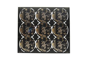
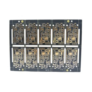
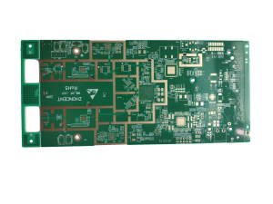
High reputation China Prototype Pcb Board - 6 Layer ENIG FR4 Heavy Copper PCB – Huihe
Crack problem of inner thick brazing pad The demand for heavy copper PCB is increasing, and the inner layer pads are getting smaller and smaller. The problem of pad cracking often occurs during PCB drilling (mainly for large holes above 2.5mm). There is little room for improvement in the material aspect of this kind of problem. The traditional improvement method is to increase the pad, increase the peeling strength of the material, and reduce the drilling rate, etc. Based on the analysis of P... -
PriceList for 4 Layer Flex Pcb - 4 Layer ENIG FR4 Heavy Copper PCB – Huihe
Heavy Copper PCB Heavy copper PCB boards can be manufactured simply by a combination of two main processes, electroplating and etching. In contrast to other PCBS, the circuit is made of a thin layer of copper foil. The heavy copper PCBs are uniformly laminated with FR4 or other epoxy-based material. The average weight of heavy copper PCBs can be 4 ounces (140μm), which is a better ratio than another common copper PCB. The additional copper thickness allows the board to conduct higher cu... -
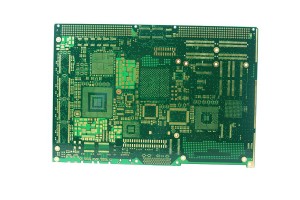
8 Year Exporter Printed Circuit Board China - 8 Layer FR4 ENIG Impedance Control PCB – Huihe
Impedance is the combination of capacitance and inductance to hinder the circuit under high frequency signal. Impedance is an AC characteristic, which means it is frequency dependent. In the case of transmitting high-frequency signals, the controlled impedance helps to ensure that there is no significant attenuation of the signal during transmission. In essence, the controlled impedance means that the material characteristics of the substrate match the characteristics of the line/dielectric l... -
Factory best selling Rigid Circuit Board - 6 Layer FR4 ENIG Impedance Control PCB – Huihe
Difference Between Pad And Via 1. Definitions Differ Pad: is the basic unit of surface mount assembly, which is used to form the landpattern of the circuit board, that is, a variety of combinations of pads designed for special component types. Through hole: through hole is also called metallization hole. In the double panel and multilayer PCB, a common hole is drilled at the junction of the wires that need to be connected between the layers in order to connect the printed wires between layers... -
Hot-selling Pcb Fab - 4 Layer ENIG FR4 Half Hole PCB – Huihe
Half Hole PCB Mainly used for on-board contact, using electroplated half-hole PCBs or castle holes, usually used when two printed circuit boards are mixed using various technologies. For example, complex modules of microcontrollers and typical single PCB configurations. Further implementations are displays, HF or concrete modules welded to the base circuit board. Therefore, the onboard PCB is required as a half coating for SMD connection pads. By connecting PCBS directly together, it is ... -
Best Price on Multi Layer Board - 14 Layer ENIG FR4 Buried Via PCB – Huihe
About Blind Buried Via PCB Blind vias and buried vias are two ways to establish connections between layers of printed circuit board. The blind vias of the printed circuit board are copper-plated vias that can be connected to the outer layer through most of the inner layer. The burrow connects two or more inner layers but does not penetrate the outer layer. Use microblind vias to increase line distribution density, improve radio frequency and electromagnetic interference, heat conduction, appl... -
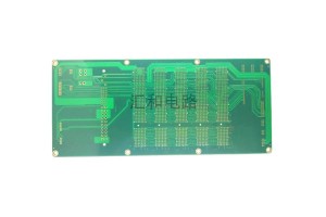
China Cheap price Fr4 Circuit Board Manufacturing - 6 Layer ENIG FR4 Blind Vias PCB – Huihe
Features Of The Blind Via PCB Blind Vias are located on the top and bottom surfaces of the circuit board and have a certain depth for the connection between the surface circuit and the inner circuit below. The depth of the hole usually does not exceed a certain ratio (aperture). This way of production will need to pay special attention to the depth of the hole (the Z axis) to the right, do not pay attention to words will cause difficult hole plating so almost no factory used, can also be conn... -
Hot sale Factory Industrial Control Pcb - 6 Layer FR4 ENIG Impedance Control PCB – Huihe
Why PCB To Do Impedance? PCB impedance refers to the resistance and the parameters of the reactance, which acts as a barrier to the alternating current. Impedance processing is essential in PCB. Here’s why: 1, PCB to consider the plug installation of electronic components, SMT patch plug also needs to consider the conductivity and signal transmission performance, so it will require the lower the impedance, the better. 2, PCB in the production process through copper deposition, electroplating ... -
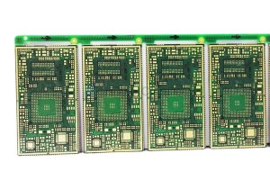
Cheap price Quick Turn Pcb Boards - 12 Layer ENIG FR4+Rogers Mixed Lamination High Frequency PCB – Huihe
Mixed Lamination High Frequency PCB Board There are three main reasons for using mixed lamination high frequency PCBs: cost, improved reliability and enhanced electrical performance. 1. Hf line materials are much more expensive than FR4. Sometimes, using mixed lamination of FR4 and hf lines can solve the cost problem. 2. In many cases, some lines of mixed lamination high frequency PCB board require high electrical performance, and some do not. 3. FR4 is used for the less electrically d... -
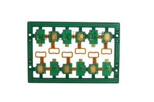
OEM/ODM Supplier Complex Circuit Board - 4 Layer FPC+FR4 Rigid Flex PCB – Huihe
Design Rules And Precautions Of Rigid Flex PCB The design of rigid flex PCB is much more complex than the traditional PCB design, and there are many places to pay attention to. In particular, the rigid flexible transition area, as well as the related wiring, through-hole design, all need to follow the requirements of the corresponding design rules. 1. Through hole position In the case of dynamic use, especially when the soft plate is often bent, the through holes on the soft plate should be a... -
Factory selling China 16 Layer Pcb Manufacture - 12 Layer ENIG FR4 Blind Vias PCB – Huihe
HDI PCB Material HDI PCB materials are RCC, LDPE, FR4 RCC:Resin coated Copper is short for resin coated copper foil. RCC is composed of copper foil and resin with rough surface, heat resistance and anti-oxidation treatment (used when the thickness is more than 4mil).The resin layer of RCC has the same processability as FR4 adhesive sheet (prepreg). In addition, it should also meet the relevant performance requirements of the laminate, such as: (1) High insulation reliability and micro via rel... -
100% Original Factory 10 Layer Pcb Fabrication - 4 Layer ENIG FR4 Half Hole PCB – Huihe
Difficulties In Machining Metallized Half-Hole PCB Metalized half-hole PCB after forming the hole wall copper black , burr residuadeviation has been a difficult problem in the molding process of PCB factoEspecially the whole row of half holes similar to stamp holes , the aperture isabout 0.6 mm , the hole wall spacing is 0.45 mm , the outer figure spacing is 2mm , because the spacing is very small , it is easy to cause short circuit because of copper skin. The general metallized half-hole PCB...


