-
China Wholesale Make Custom Pcb Manufacturers - 6 Layer ENIG Impedance Control PCB 14706 – Huihe
Difference between pad and via 1. Definitions differ Pad: is the basic unit of surface mount assembly, which is used to form the landpattern of the circuit board, that is, a variety of combinations of pads designed for special component types. Through hole: through hole is also called metallization hole. In the double panel and multilayer PCB, a common hole is drilled at the junction of the wires that need to be connected between the layers in order to connect the printed wires between l... -
China Wholesale Printed Circuit Board Components Pricelist - 10 Layer Medium TG Gold Finger PCB – Huihe
The advantages of high Tg materials The main advantage of high Tg materials is higher operating temperature( MOT ) , which can carry more current . According to experience , TG minusabout 20 C can be used as mot . At this temperature , the PCB can runnormally for a long time without damage. The heat resistance temperature of the common solder mask is usually lowerthan the Tg of the substrate . The conventional maximum operatingtemperature of solder mask is about 150 C . For high Tg appli... -
China Wholesale Hitech Pcb Suppliers - 2 layer ENIG Heavy Copper PCB 15872 – Huihe
Difficulties in drilling heavy copper PCBs With the increase of the copper thickness, the thickness of the heavy copper PCB also increases. heavy copper PCB is usually more than 2.0mm thick, drilling production due to the thickness of the thickness of the plate and copper thick factors, production is more difficult. In this regard, the use of a new cutter, reduce the service life of the drill cutter, section drilling has become an effective solution to the heavy copper PCB drilling. In a... -
China Wholesale Multilayer Flex Pcb Manufacturers - 14 Layer High TG Fine Pitch PCB 14 – Huihe
About High Tg PCB The general TG is more than 130 degrees, the high Tg is more than 170 degrees, and the medium TG is more than 150 degrees. Generally, PCB with TG ≥ 170 ℃ is called high Tg PCB. When the Tg of the substrate is increased, the heat resistance, moisture resistance, chemical resistance, stability resistance and other characteristics of the circuit board will be improved. The higher the TG value, the better the temperature resistance of the sheet, especially in the lead-free ... -
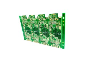
China Wholesale Simple Pcb Board Manufacturers - 6 Layer ENIG Impedance Control PCB 14706 – Huihe
Difference between pad and via 1. Definitions differ Pad: is the basic unit of surface mount assembly, which is used to form the landpattern of the circuit board, that is, a variety of combinations of pads designed for special component types. Through hole: through hole is also called metallization hole. In the double panel and multilayer PCB, a common hole is drilled at the junction of the wires that need to be connected between the layers in order to connect the printed wires between l... -
China Wholesale Electronic Circuit Board Assembly Suppliers - 6 Layer ENIG Impedance Control PCB 14706 – Huihe
Difference between pad and via 1. Definitions differ Pad: is the basic unit of surface mount assembly, which is used to form the landpattern of the circuit board, that is, a variety of combinations of pads designed for special component types. Through hole: through hole is also called metallization hole. In the double panel and multilayer PCB, a common hole is drilled at the junction of the wires that need to be connected between the layers in order to connect the printed wires between l... -
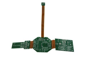
China Wholesale Circuit Board Assembly Quotes - 4 Layer FPC+FR4 Rigid-Flex PCB – Huihe
About the Rigid-Flex PCB Rigid-Flex PCB, is the flexible PCB and traditional Rigid PCB, after many procedures, according to the relevant process requirements combined together, forming at the same time with FPC characteristics and PCB characteristics of the circuit board. It can be used in some products with special requirements, both a certain flexible area and a certain rigid area, to save the internal space of the product, reduce the volume of finished products, improve the performance of ... -

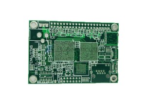
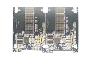
China Wholesale Driver Pcb Factories - 8 Layer ENIG Blind Buried Via PCB 12 – Huihe
About Level 1 Level 1 HDI technology refers to the laser blind hole only connected to the surface layer and its adjacent secondary layer hole forming technology. pressing in one time after drilling →utside again pressing copper foil → and then laser drilling About Level 1 Level 2 HDI PCB The Level 2 HDI technology is an improvement on the Level 1 HDI technology. It includes two forms of laser blind via drilling directly from the surface layer to the third layer, and laser blind... -
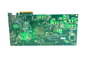
China Wholesale Non Printed Circuit Board Quotes - 6 Layer ENIG Impedance Control PCB 8931 – Huihe
Impedance characteristics of PCB According to the signal transmission theory, the signal is a function of time and distance variables, so every part of the signal on the line may change. Therefore, the AC impedance of the transmission line, that is, the ratio of voltage change to current change, is determined as the characteristic impedance of the transmission line. The characteristic impedance of the transmission line is only related to the characteristics of the signal connection itsel... -
China Wholesale Best Pcb Suppliers - 10 Layer Medium TG Gold Finger PCB – Huihe
The advantages of high Tg materials The main advantage of high Tg materials is higher operating temperature( MOT ) , which can carry more current . According to experience , TG minusabout 20 C can be used as mot . At this temperature , the PCB can runnormally for a long time without damage. The heat resistance temperature of the common solder mask is usually lowerthan the Tg of the substrate . The conventional maximum operatingtemperature of solder mask is about 150 C . For high Tg appli... -
China Wholesale Pcb Producer Quotes - 4 Layer FR4+Rogers PCB 28848 – Huihe
The difficulty of laminated structure of mixed press PCB One of the major challenges in RF/microwave applications is how to ensure that the actual tolerances are within the design tolerances, so as to achieve the desired operating frequency. One of the biggest challenges in the lamination design of mixed-pressure structures is to have uniform thickness between different panels or even between different pieces. Due to the existence of a variety of substrate material types, there are a variety ... -
China Wholesale Rigid Flex Circuit Boards Suppliers - 6 Layer ENIG via-in-pad PCB 16842 – Huihe
The advantages and disadvantages of plugging and no plugging? In terms of plug holes, they have the following advantages 1. the plug hole can prevent PCB through the wave soldering tin from the through hole through the component surface caused by short circuit; That is to say, within the scope of the wave soldering design area (generally the welding surface is 5mm or above) there is no hole or hole to do plug hole treatment. 2. The plug hole protects against possible short circuits caused by ...


