-
China Wholesale Hal Pcb Suppliers - 6 Layer ENIG Impedance Control PCB 7736 – Huihe
Why PCB to do impedance? PCB impedance refers to the resistance and the parameters of the reactance, which acts as a barrier to the alternating current. Impedance processing is essential in PCB. Here’s why: 1, PCB to consider the plug installation of electronic components, SMT patch plug also needs to consider the conductivity and signal transmission performance, so it will require the lower the impedance, the better. 2, PCB in the production process through copper deposition, electroplating ... -
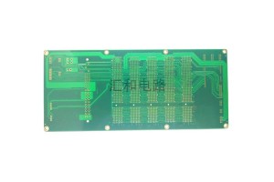
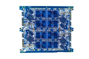
China Wholesale Pcb Order Suppliers - 6 Layer ENIG Impedance Control PCB 9806 – Huihe
About the impedance Impedance is the combination of capacitance and inductance to block the circuit in high frequency signal. Impedance is a kind of AC characteristic, which means that it is related to frequency and is used to describe the high frequency characteristics of PCB. Factors affecting impedance DK (R): determined by raw materials (PCB material, semi cured sheet) Line thickness (T): determined by raw materials and process capability. Line width (W): determined by customer’... -
China Wholesale Load Board Pcb Suppliers - 4 Layer OSP Impedance Control PCB 8742 – Huihe
Characteristic impedance control of PCB The characteristic impedance of the conductor on thePCB is an important index of circuit design, especially in the PCB design of high frequency circuit, we must consider whether the characteristic impedance of the conductor is consistent with the characteristic impedance required by the device or signal. PCB impedance matching In the PCB, if there is a signal transmission, it is expected to be from the sending end of the power supply, in the c... -

China Wholesale Flex Printed Circuit Board Pricelist - 6 Layer ENIG Impedance Control PCB 10222 – Huihe
Factors determining controlled impedance The characteristic impedance of a PCB is usually determined by its inductance and capacitance, resistance and conductance. These factors are functions of the physical size of the circuit, the dielectric constant and dielectric thickness of the PCB substrate material. In general, the line impedance of a PCB ranges from 25 to 125Ω. The PCB structure that determines the impedance value consists of the following factors: Width and thickness of top and... -
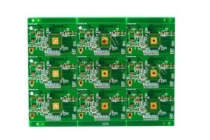
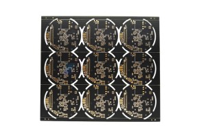
China Wholesale Circular Circuit Board Quotes - 8 Layer impedance ENIG PCB 6351 – Huihe
Half hole technology After the PCB is made in the half hole, the tin layer is set at the edge of the hole by electroplating. The tin layer is used as the protective layer to enhance the tear resistance and completely prevent the copper layer falling off from the hole wall. Therefore, the impurity generation in the production process of the printed circuit board is reduced, and the workload of cleaning is also reduced, so as to improve the quality of the finished PCB. After the production... -

China Wholesale Mini Pcb Board Quotes - 6 layer ENIG Impedance Control Heavy Copper PCB 15881 – Huihe
Functions of heavy copper PCB Heavy copper PCB has the best extension functions, is not limited by the processing temperature, high melting point can be used oxygen blowing, low temperature at the same brittle and other hot melt welding, but also fire prevention, belongs to the non-combustible material. Even in highly corrosive atmospheric conditions, copper sheets form a strong, non-toxic passivation protective layer. Difficulty in machining control of heavy copper PCB Thickness of copper PC... -
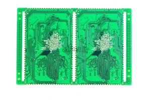
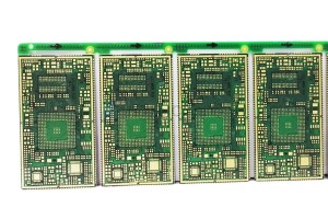
China Wholesale High Current Pcb Suppliers - 6-layer ENIG impedance control PCB 15749 – Huihe
Differences between multilayer PCB and single panel / double-sided PC The biggest difference between multilayer PCB and single panel and double panel is that the internal power supply layer (to maintain the internal power layer) and the ground layer are added. The power supply and ground wire network are mainly wired on the power supply layer. However, the multilayer wiring is mainly the top and bottom layer, with the middle wiring layer as a supplement. Therefore, the design method of m... -
China Wholesale Emc Pcb Manufacturers - 6 layer ENIG Heavy Copper PCB 15202 – Huihe
Crack problem of inner thick brazing pad The demand for heavy copper PCB is increasing, and the inner layer pads are getting smaller and smaller. The problem of pad cracking often occurs during PCB drilling (mainly for large holes above 2.5mm). There is little room for improvement in the material aspect of this kind of problem. The traditional improvement method is to increase the pad, increase the peeling strength of the material, and reduce the drilling rate, etc. Based on the analysis... -
China Wholesale Matte Black Pcb Factories - 6 Layer ENIG Blind Vias PCB 27809 – Huihe
Features of the Blind Via Blind Vias are located on the top and bottom surfaces of the circuit board and have a certain depth for the connection between the surface circuit and the inner circuit below. The depth of the hole usually does not exceed a certain ratio (aperture). This way of production will need to pay special attention to the depth of the hole (the Z axis) to the right, do not pay attention to words will cause difficult hole plating so almost no factory used, can also be connecte... -

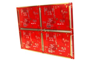
China Wholesale Pcb Clad Board Quotes - 8 Layer ENIG Blind Buried Via PCB 12 – Huihe
About Level 1 Level 1 HDI technology refers to the laser blind hole only connected to the surface layer and its adjacent secondary layer hole forming technology. pressing in one time after drilling →utside again pressing copper foil → and then laser drilling About Level 1 Level 2 HDI PCB The Level 2 HDI technology is an improvement on the Level 1 HDI technology. It includes two forms of laser blind via drilling directly from the surface layer to the third layer, and laser blind... -
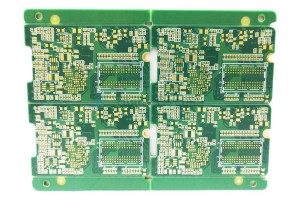
China Wholesale Populated Printed Circuit Boards Pricelist - 10 Layer ENIG Blind Vias PCB 28526 – Huihe
About Blind Buried Via PCB Blind Via: which enables the connection and conduction between the inner and outer layers Buried Via: which can connect and guide between inner layers Blind Vias are mostly small holes with a diameter of 0.05mm~0.15mm. There are laser hole forming, plasma etched hole and photoinduced hole forming, and laser hole forming is usually used. HDI: High-density interconnection, non-mechanical drilling, micro-blind hole ring below 6mil, inside and outside layers of wiring l... -

China Wholesale Pcb Bare Board Quotes - 6 Layer Rogers+ FR4 PCB – Huihe
The electrical, thermal and mechanical properties of high-frequency materials are different from those of conventional FR-4 materials. High frequency PCB has low dielectric constant Dk, low transmission delay, low loss factor Df and low dielectric loss. The high-frequency microwave board and RF board produced by Huihe Circuit include 5G base station antenna circuit board, 4G intermodulation antenna circuit board, high-precision impedance circuit board, high-frequency high-speed mixed voltage ...


