-
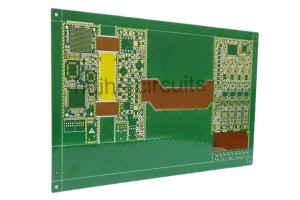
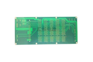
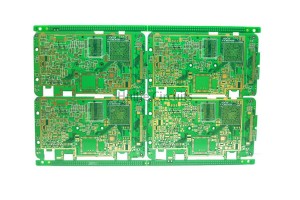
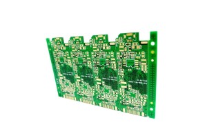
China Wholesale Pcb Tg Quotes - 8 Layer FPC+FR4 Rigid-Flex PCB 8 – Huihe
Rigid-Flex PCB in consumer electronic products The first use of Rigid-Flex PCB in the field of battery modules, now look at all mobile phone brands around the world, the use of Rigid-Flex PCB battery has been a consensus, and may become a long-term trend. At the same time, in order to accommodate more lenses in smaller and smaller space, mobile phone lens module also began to use the Rigid-Flex PCB, in addition to gradually expanded to display and other mobile phone modules. As for the l... -
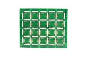
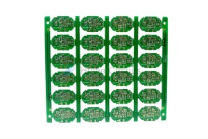
China Wholesale Rigid Flex Printed Circuit Boards Quotes - 10 Layer ENIG Blind Vias PCB 28526 – Huihe
About Blind Buried Via PCB Blind Via: which enables the connection and conduction between the inner and outer layers Buried Via: which can connect and guide between inner layers Blind Vias are mostly small holes with a diameter of 0.05mm~0.15mm. There are laser hole forming, plasma etched hole and photoinduced hole forming, and laser hole forming is usually used. HDI: High-density interconnection, non-mechanical drilling, micro-blind hole ring below 6mil, inside and outside layers of wiring l... -
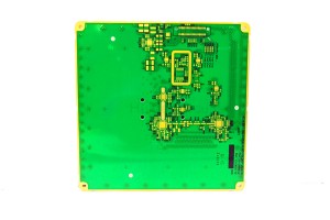
China Wholesale Laser Circuit Board Pricelist - 6 Layer ENIG via-in-pad PCB 16942 – Huihe
How to understand half plug hole and full plug hole The whole plug hole is the whole through hole is blocked by green oil. Generally, TOP and BOT fill the hole with green oil on both sides, and the fullness is more than 80%. The half plug hole refers to the plug from one side, opaque, half plug hole, fullness is not good control, general factory can only do about 30-50%, according to the factory’s own ability, mainly used in, one side of the window, one side of the window area, such as s... -
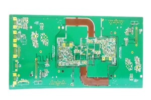
China Wholesale Pcb Custom Order Pricelist - 8 Layer ENIG Impedance Control PCB 16978 – Huihe
Deficiencies of the blind buried vias The main problem of blind buried via is the high cost. In contrast, buried holes cost less than blind holes, but the use of both types of holes can significantly increase the cost of a board. The cost increase is due to the more complex manufacturing process of the blind buried hole, that is, the increase in manufacturing processes also leads to the increase in testing and inspection processes. Buried Via Buried vias are used to connect differen... -
China Wholesale Small Prototype Board Suppliers - 6 Layer ENIG Impedance Control PCB 7736 – Huihe
Why PCB to do impedance? PCB impedance refers to the resistance and the parameters of the reactance, which acts as a barrier to the alternating current. Impedance processing is essential in PCB. Here’s why: 1, PCB to consider the plug installation of electronic components, SMT patch plug also needs to consider the conductivity and signal transmission performance, so it will require the lower the impedance, the better. 2, PCB in the production process through copper deposition, electroplating ... -
China Wholesale Electronic Circuit Board Assembly Quotes - 4 Layer ENIG half hole PCB – Huihe
Difficulties in machining metallized half-hole PCB Metalized half-hole PCB after forming the hole wall copper black , burr residuadeviation has been a difficult problem in the molding process of PCB factoEspecially the whole row of half holes similar to stamp holes , the aperture isabout 0.6 mm , the hole wall spacing is 0 . 45 mm , the outer figure spacing is 2mm , because the spacing is very small , it is easy to cause short circuitbecause of copper skin. The general metallized half-ho... -
China Wholesale Rf Circuit Board Manufacturers - 6 Layer FR4+Rogers PCB 28727 – Huihe
Features of high frequency PCB 1. High frequency PCB with small dielectric constant, loss will be very small, and advanced induction heating technology can achieve the needs of the target heating, very high efficiency. Of course, while paying attention to efficiency, it also has the characteristics of environmental protection, which is very suitable for the development direction of today’s society. 2. The transmission speed is inversely proportional to the square root of the dielec... -
China Wholesale Pcb Board Supplier Manufacturers - 8 Layer FPC+FR4 Rigid Flex PCB 4 – Huihe
The Rigid Flex PCB plays a key role in the automotive market The Rigid Flex PCB is becoming more and more important in automotive electronics, which is beyond PCB operators’ original imagination. The reason is that we did not think that the technology used in mobile phone lens module would have the opportunity to extend to the ADAS lens module for car, and further attract the auto component industry to introduce the Rigid Flex PCB into the module products such as photar, and become the entry ... -

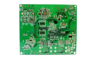
China Wholesale Laser Circuit Board Suppliers - 8 layer ENIG Impedance Control Heavy Copper PCB 16555 – Huihe
Thin core heavy copper PCB copper foil choice The most concerned problem of heavy copper CCL PCB is the pressure resistance problem, especially the thin core heavy copper PCB (thin core is medium thickness ≤ 0.3mm), the pressure resistance problem is particularly prominent, thin core heavy copper PCB will generally choose RTF copper foil for production, RTF copper foil and STD copper foil main difference is the length of the wool Ra is different, RTF copper foil Ra is significantly less ... -
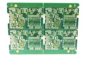
China Wholesale Order Printed Circuit Board Suppliers - 8 layer ENIG impedance control PCB 14911 – Huihe
Challenges of the multilayer PCB Multilayer PCB designs are more expensive than other types. There are some usability issues. Because of its complexity, the production time is quite long. Professional designer who needs to manufacture multilayer PCB. The main features of multilayer PCB 1. Used with integrated circuit, it is conducive to miniaturization and weight reduction of the whole machine; 2. Short wiring, straight wiring, high wiring density; 3. Because the shielding layer is ... -
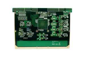
China Wholesale Printed Wiring Board Assembly Manufacturers - 6 Layer ENIG Impedance Control PCB 14706 – Huihe
Difference between pad and via 1. Definitions differ Pad: is the basic unit of surface mount assembly, which is used to form the landpattern of the circuit board, that is, a variety of combinations of pads designed for special component types. Through hole: through hole is also called metallization hole. In the double panel and multilayer PCB, a common hole is drilled at the junction of the wires that need to be connected between the layers in order to connect the printed wires between l... -
China Wholesale Production Of Pcb Pricelist - 6 Layer ENIG via-in-pad PCB 16842 – Huihe
The advantages and disadvantages of plugging and no plugging? In terms of plug holes, they have the following advantages 1. the plug hole can prevent PCB through the wave soldering tin from the through hole through the component surface caused by short circuit; That is to say, within the scope of the wave soldering design area (generally the welding surface is 5mm or above) there is no hole or hole to do plug hole treatment. 2. The plug hole protects against possible short circuits caused by ...


