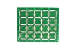
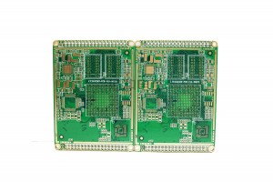
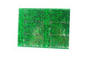
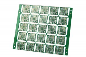
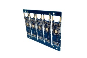
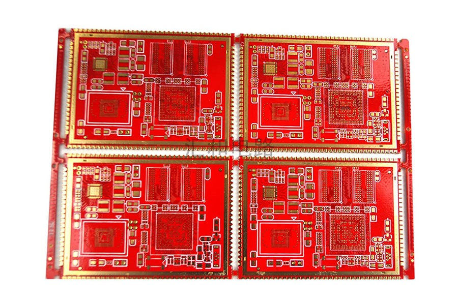
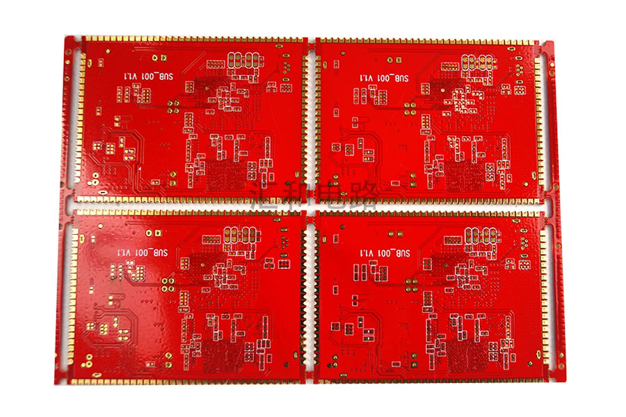
8 Layer impedance ENIG PCB 6351
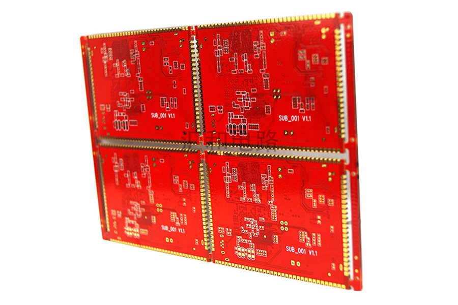
Half Hole Technology
After the PCB is made in the half hole, the tin layer is set at the edge of the hole by electroplating. The tin layer is used as the protective layer to enhance the tear resistance and completely prevent the copper layer falling off from the hole wall. Therefore, the impurity generation in the production process of the printed circuit board is reduced, and the workload of cleaning is also reduced, so as to improve the quality of the finished PCB.
After the production of conventional half-hole PCB is completed, there will be copper chips on both sides of the half-hole, and the copper chips will be involved in the inner side of the half-hole. Half hole is used as a child PCB, the role of the half hole is in the process of PCBA, will take half a child of the PCB, by giving half a hole filling of tin to make half the master plate welded on the main board, and half a hole with copper scrap, will directly affect tin, affecting the welding firmly of the sheet on the motherboard, and affect the appearance and the use of the whole machine performance.
The surface of the half hole is provided with a metal layer, and the intersection of the half hole and the edge of the body is respectively provided with a gap, and the surface of the gap is a plane or the surface of the gap is a combination of the plane and the surface of the surface. By increasing the gap at both ends of the half hole, the copper chips at the intersection of the half hole and the body edge are removed to form a smooth PCB, effectively avoiding the copper chips remaining in the half hole, ensuring the quality of the PCB , as well as the reliable welding and appearance quality of the PCB in the process of PCBA, and ensuring the performance of the whole machine after subsequent assembly.
Equipment Display

PCB Automatic Plating Line

PCB PTH Line

PCB LDI

PCB CCD Exposure Machine
Factory Show

PCB Manufacturing Base

Admin Receptionist

Meeting Room