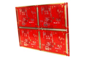
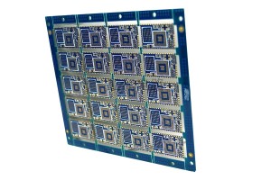
4 Layer ENIG FR4 Half Hole PCB
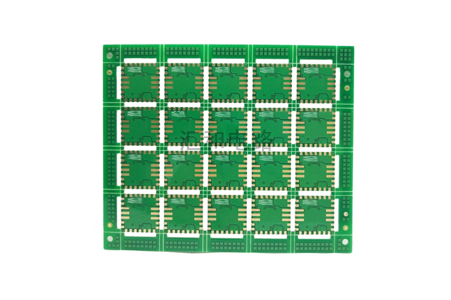

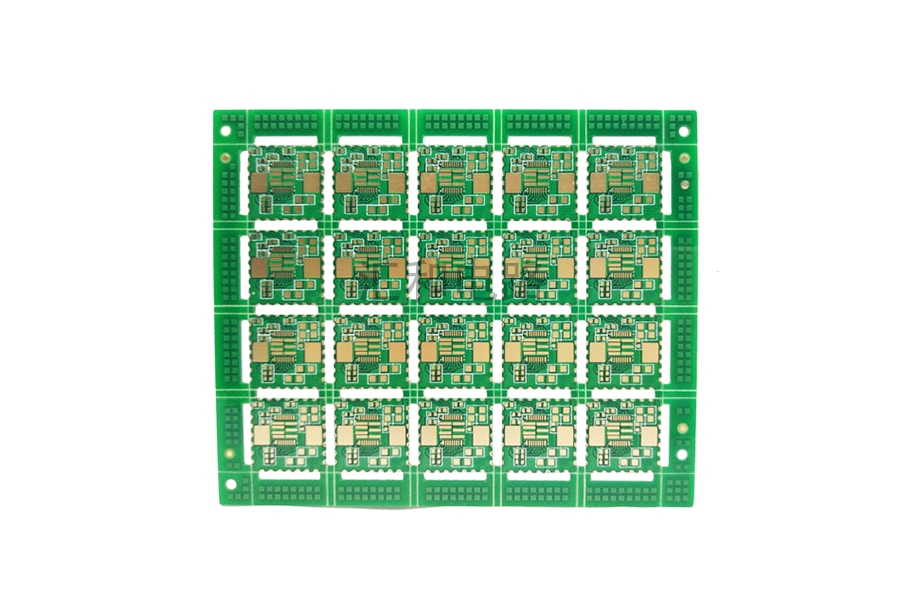
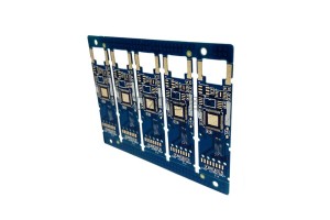
Half Hole PCB Splicing Method
By using the stamp hole splicing method, the purpose is to make the connecting bar between the small plate and the small plate. In order to facilitate the cutting, some holes will be opened on the top of the bar (the diameter of the conventional hole is 0.65-0.85 MM), which is the stamp hole. Now the board has to pass the SMD machine, so when you do the PCB, you can connect the board too many PCB. at a time After the SMD, the back board should be separated, and the stamp hole can make the board easy to separate. The half-hole edge can not be cut V forming, gong empty (CNC) forming.
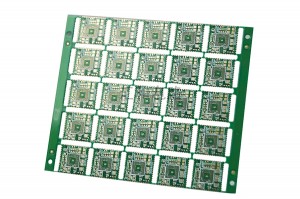
1.V-cutting splicing plate, half hole PCB edge do not do V-cutting forming (will pull copper wire, resulting in no copper hole)
2. Stamp Set
The PCB splicing method is mainly V-CUT、bridge connection, bridge connection stamp hole these several ways, the splice size can not be too big, also can not be too small, generally very small board can splice the plate processing or the convenient welding but splice the PCB.
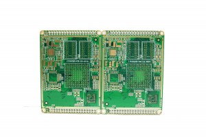
In order to control the production of metal half-hole plate, some measures are usually taken to cross the hole wall copper skin between metallized half-hole and nonmetallic hole due to technological problems. Metalized half-hole PCB is relatively PCB in various industries. The metallized half hole is easy to pull out the copper in the hole when milling the edge, so the scrap rate is very high. For drape internal turning, the prevention product must be modified in the later process because of the quality. The process of making this type of plate is treated according to the following procedures: drilling (drilling, gong groove, plate plating, external light imaging, graphic electroplating, drying, half hole treatment, film removal, etching, tin removal, other processes, shape).
Equipment Display

PCB Automatic Plating Line

PCB PTH Line

PCB LDI

PCB CCD Exposure Machine
Factory Show

PCB Manufacturing Base

Admin Receptionist

Meeting Room