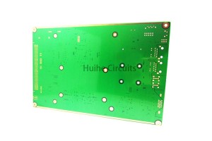
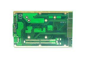
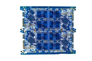
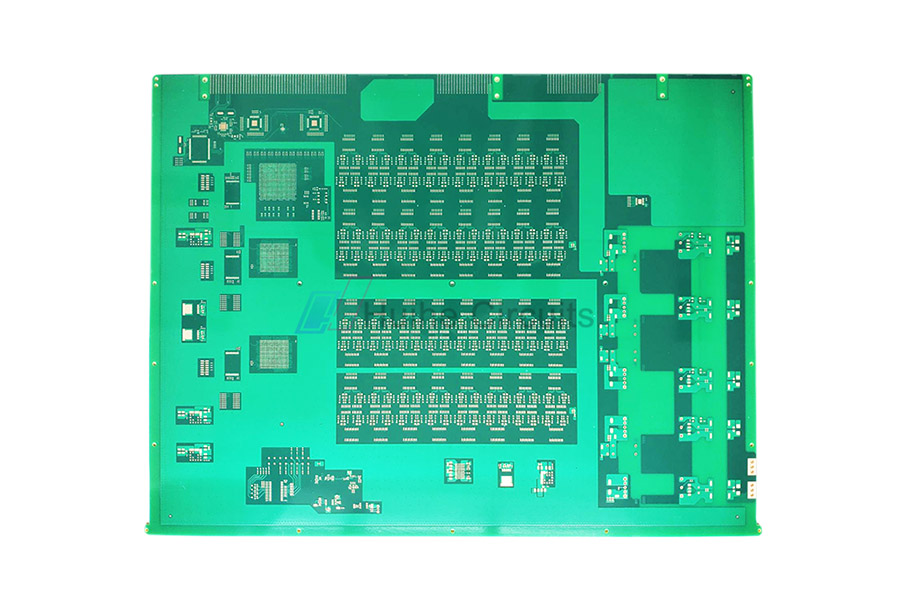
10 Layer ENIG Impedance Control PCB
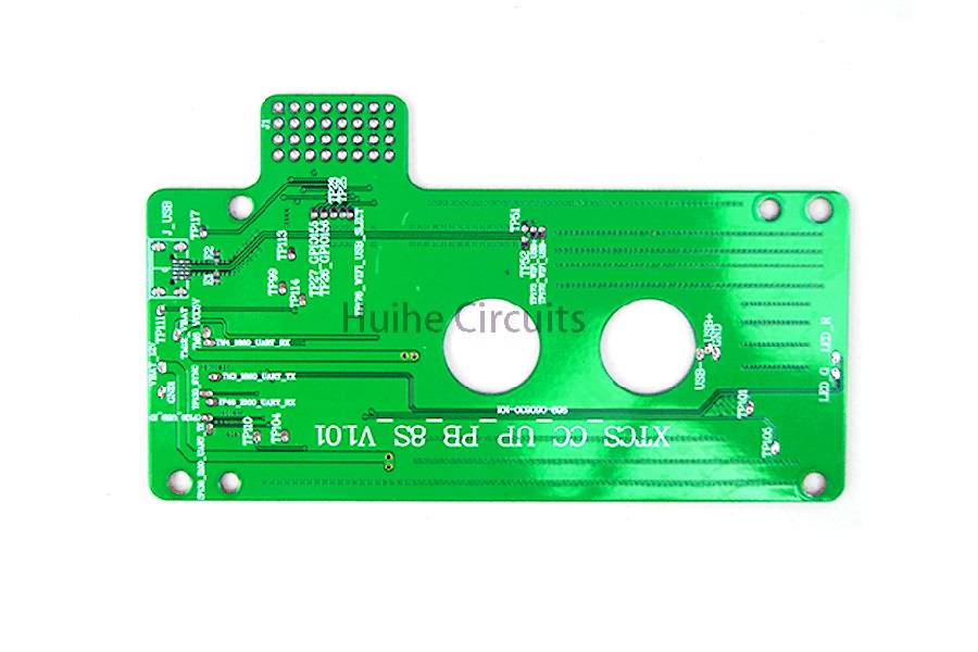
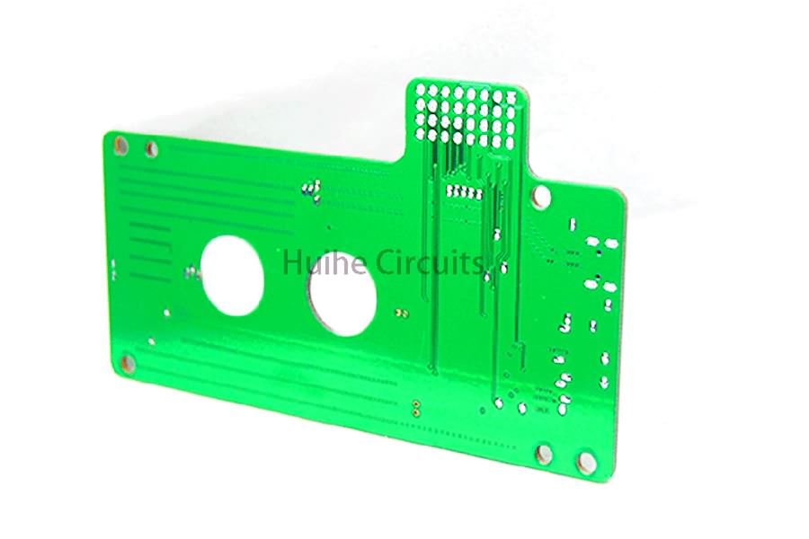
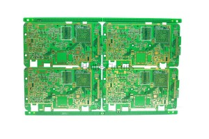
About Multilayer PCB
Multilayer PCB refers to the multilayer PCB used in electrical products, multilayer board using more single or double panel wiring board. With a double lining, two one-way for outer layer or two double lining, two blocks of single outer layer of the printed circuit board, through the positioning and alternate insulation adhesive materials and conductive graphics interconnection according to design requirement of printed circuit board becomes four, six layer PCB, also known as multilayer PCB.
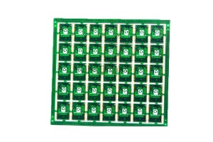
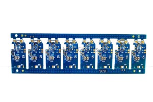
A Variety Of PCB Processes
Impedance Control PCB
Strictly control the conductor width/thickness and medium thickness
Impedance linewidth tolerance ≤± 5%, good impedance matching
Applied to high-frequency and high-speed devices and 5g communication equipment
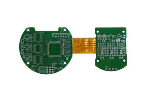
Rigid-Flex PCB
Flexible and thin, simplifying the product assembly process
Reduce connectors, high line carrying capacity
Used in image system and RF communication equipment
Via-in-Pad PCB
Use electroplating to fill holes/resin plug holes
Avoid solder paste or flux flowing into pan holes
Prevent holes with tin beads or ink pad lead to weld
Bluetooth module for consumer electronics industry
Heavy Copper PCB
Copper can be up to 12 OZ and has a high current
The material is FR-4/Teflon/ceramic
Applied to high power supply, motor circuit
Equipment Display

PCB Automatic Plating Line

PCB PTH Line

PCB LDI

PCB CCD Exposure Machine
Factory Show

PCB Manufacturing Base

Admin Receptionist

Meeting Room