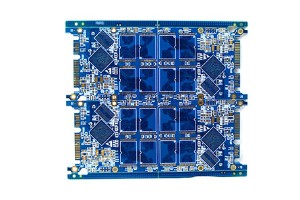
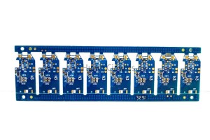
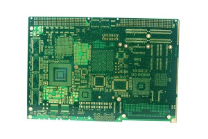
6 Layer ENIG Impedance Control PCB
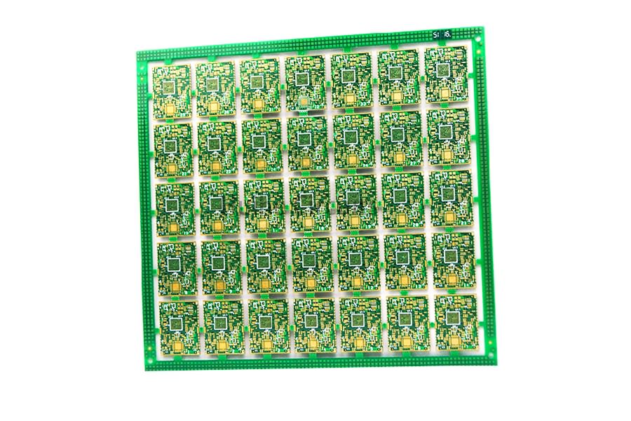
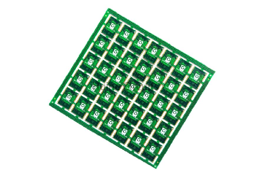
About Multilayer PCB
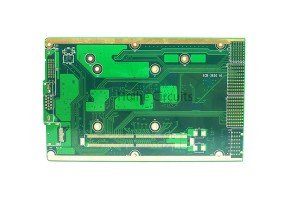
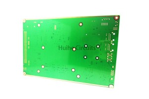
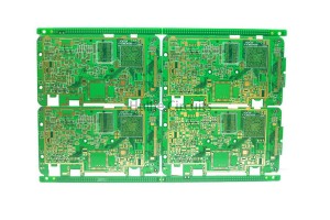
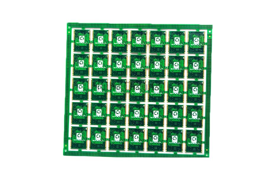
With the increasing complexity of circuit design, in order to increase the area of wiring, multilayer PCB can be used. Multilayer board is a PCB that contains multiple working layers. In addition to the top and bottom layers, it also includes signal layer, middle layer, internal power supply and ground layer.
The number of layers of PCB represents that there are several independent wiring layers. Generally, the number of layers is even and includes the outermost two layers. Because it can make full use of multilayer board to solve the problem of electromagnetic compatibility, it can greatly improve the reliability and stability of the circuit, so the application of multilayer board is more and more widely.
PCB Transaction Process
A Variety Of PCB Processes
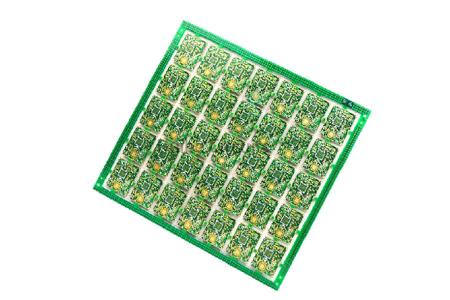
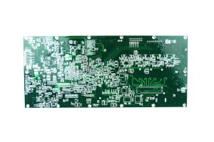
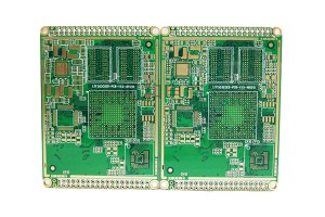
Multilayer PCB
Minimum line width and line spacing 3/3mil
BGA 0.4pitch, minimum hole 0.1mm
Used in industrial control and consumer electronics
Half Hole PCB
There is no residual or warping of copper thorn in half hole
The child board of the mother board saves connectors and space
Applied to Bluetooth module, signal receiver
Blind Buried Via PCB
Use micro-blind holes to increase the line density
Improve radio frequency and electromagnetic interference, heat conduction
Apply to servers, mobile phones, and digital cameras
Via-in-Pad PCB
Use electroplating to fill holes/resin plug holes
Avoid solder paste or flux flowing into pan holes
Prevent holes with tin beads or ink pad lead to weld
Bluetooth module for consumer electronics industry
Write your message here and send it to us