
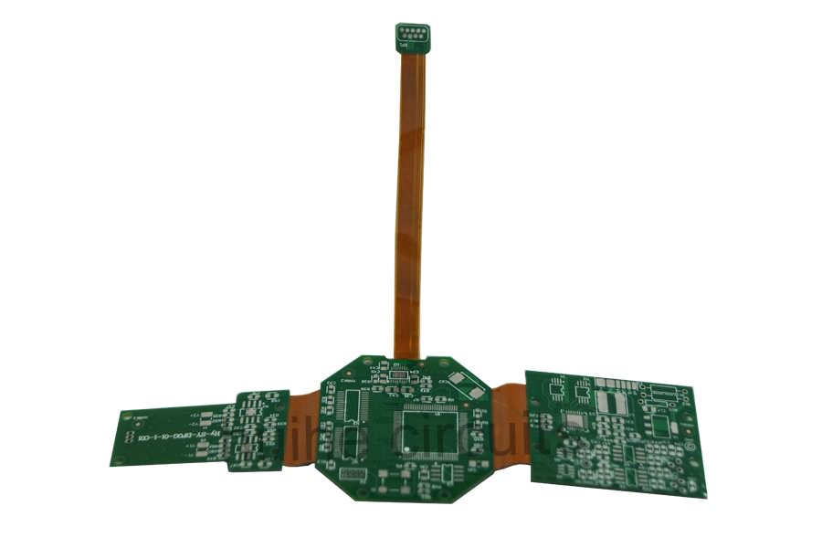
Professional Design Flex Pcb Prototype - 6 Layer ENIG Via-In-Pad PCB – Huihe
Professional Design Flex Pcb Prototype - 6 Layer ENIG Via-In-Pad PCB – Huihe Detail:
Advantages Of The Plug Hole
1. The plug hole can prevent PCB through the wave soldering tin from the through hole through the component surface caused by short circuit; That is to say, within the scope of the wave soldering design area (generally the welding surface is 5mm or above) there is no hole or hole to do plug hole treatment. 2. The plug hole protects against possible short circuits caused by closely spaced devices such as BGA. This is the reason for the hole under the BGA to keep the hole in the design process. Because there is no plug hole, this is a case of short circuit. 3. Avoid flux residue in the conduction hole; 4. After the surface mounting and component assembly of the electronics factory is completed, the PCB shall be vacuum absorbed and negative pressure formed on the test machine before completion: 5. Prevent the surface solder paste into the hole caused by virtual welding, affect the installation; This point is most obvious in the heat dissipation pad with holes. 6. To prevent the wave soldering tin beads pop up, resulting in a short circuit. 7. The plug hole will be helpful to the SMT process.
Equipment Display

PCB Automatic Plating Line

PCB PTH Line

PCB LDI

PCB CCD Exposure Machine
Factory Show

PCB Manufacturing Base

Admin Receptionist

Meeting Room

General Office
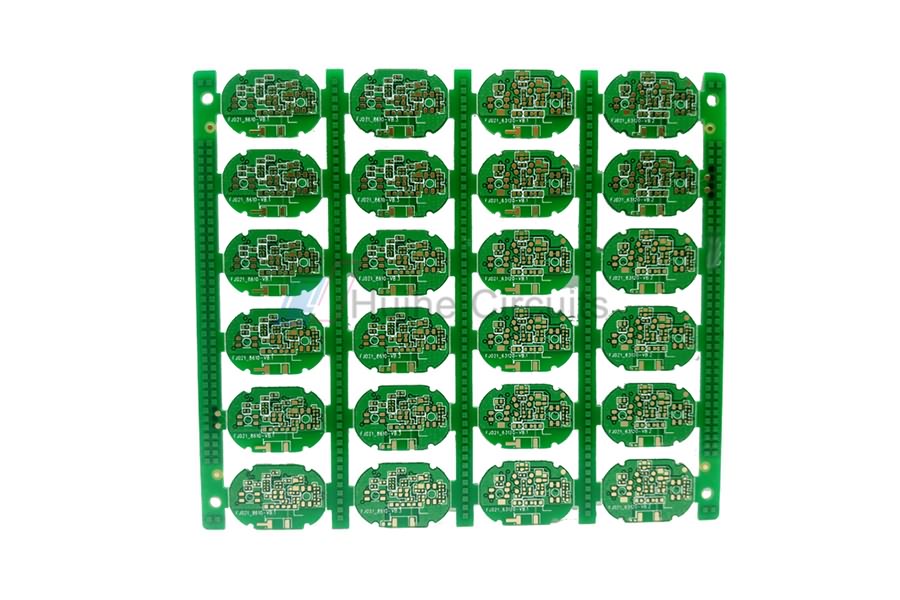
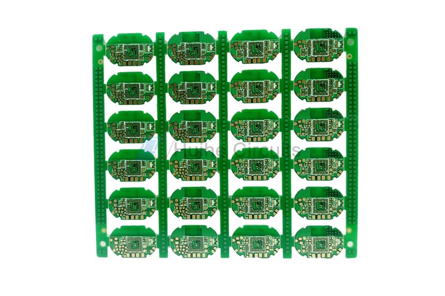
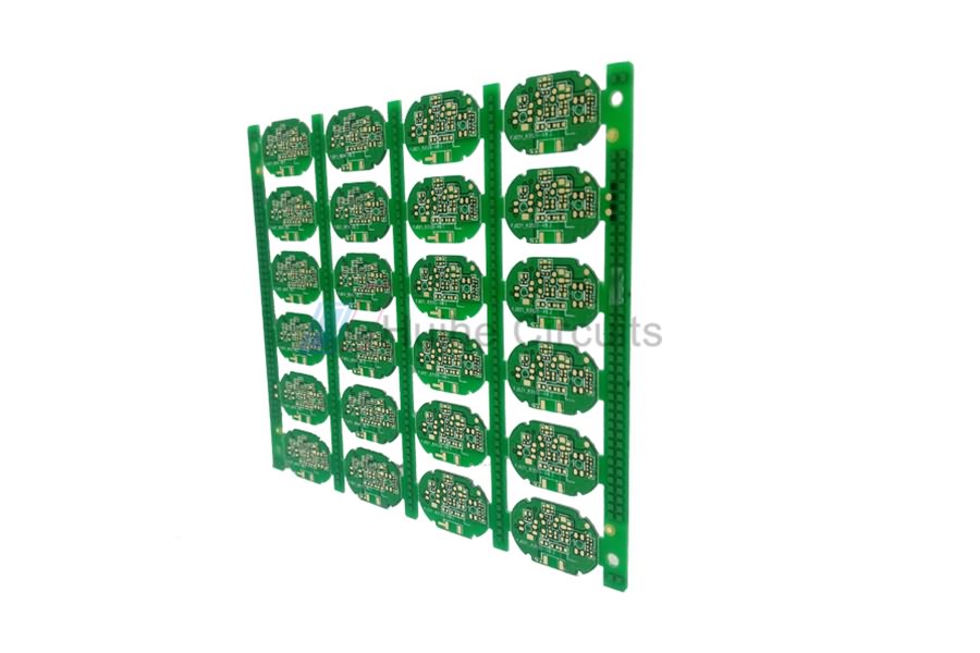
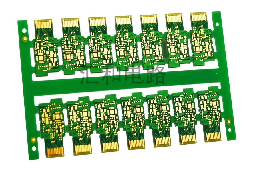
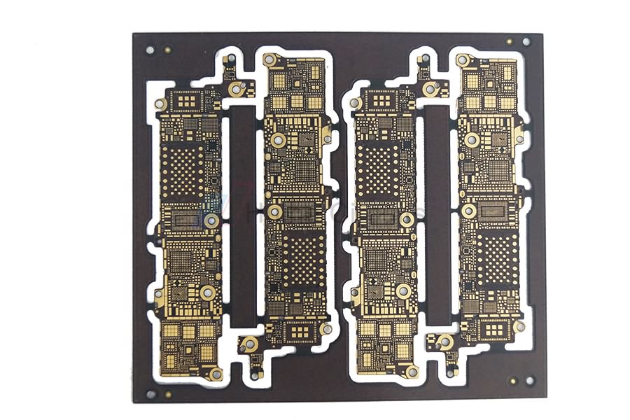
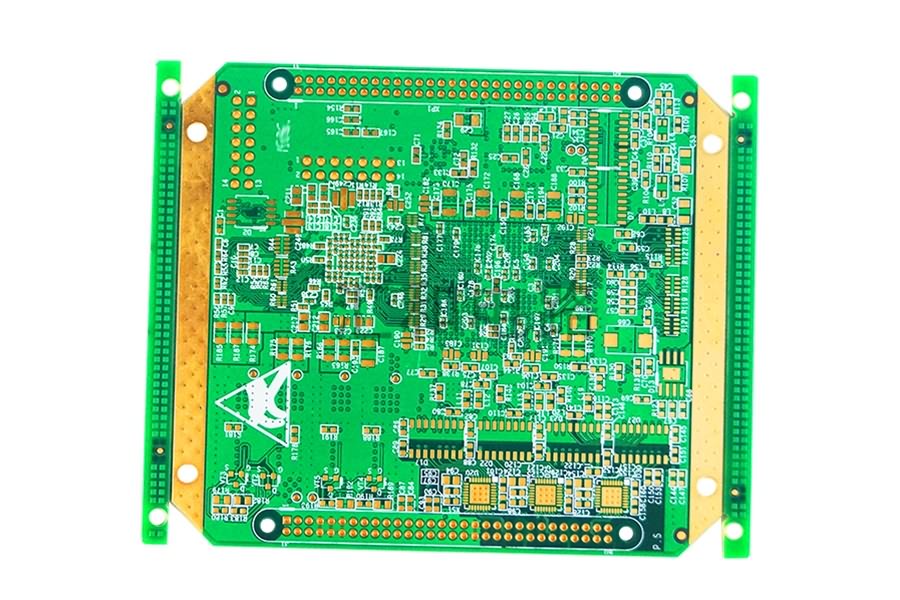
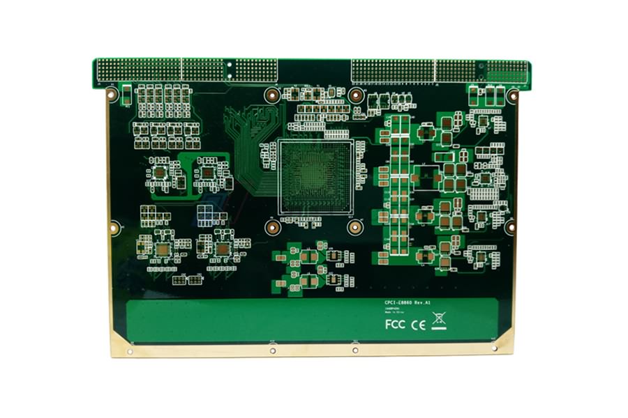
Product detail pictures:
Related Product Guide:
With our abundant experience and considerate products and services, we have been recognized to be a reputable supplier for a lot of global consumers for Professional Design Flex Pcb Prototype - 6 Layer ENIG Via-In-Pad PCB – Huihe , The product will supply to all over the world, such as: Slovak Republic, Madagascar, Yemen, Welcome to visit our company and factory, there are various products displayed in our showroom that will meet your expectation, meanwhile, if you are convenient to visit our website, our sales staff will try their efforts to provide you the best service
Production management mechanism is completed, quality is guaranteed, high credibility and service let the cooperation is easy, perfect!
-
China Wholesale Non Printed Circuit Board Price...
-
China Wholesale Wifi Pcb Board Manufacturers -...
-
Free sample for Custom Circuit Board Printing -...
-
Factory Price For China Rohs Pcb - 8 Layer ENI...
-
China Wholesale Turnkey Pcb Pricelist - 4 Laye...
-

China Supplier Pcb Board Supplier In China - 4...


