
China Wholesale Wifi Pcb Board Manufacturers - 8 Layer ENIG Blind Buried Via PCB – Huihe
China Wholesale Wifi Pcb Board Manufacturers - 8 Layer ENIG Blind Buried Via PCB – Huihe Detail:
About Level 1 HDI PCB
Level 1 HDI PCB technology refers to the laser blind hole only connected to the surface layer and its adjacent secondary layer hole forming technology.
pressing in one time after drilling →utside again pressing copper foil → and then laser drilling

About Level 1 HDI PCB
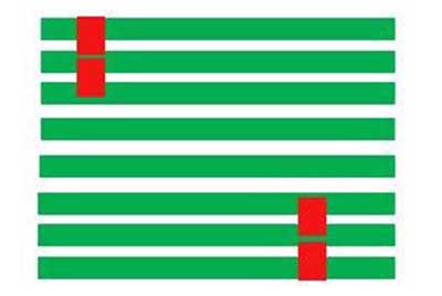
Level 2 HDI PCB
The Level 2 HDI PCB technology is an improvement on the Level 1 HDI PCB technology. It includes two forms of laser blind via drilling directly from the surface layer to the third layer, and laser blind hole drilling directly from the surface layer to the second layer and then from the second layer to the third layer. The difficulty of the Level 2 HDI PCB technology is far greater than the Level 1 HDI PCB technology.
Press in one time after drilling →outside again pressing copper foil →laser, drilling→outer again pressing copper foil→ laser drilling
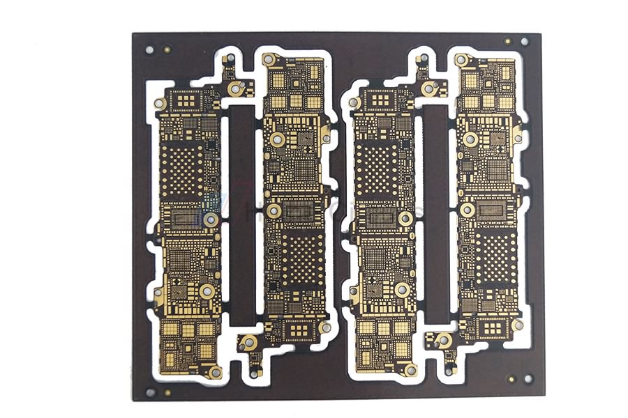
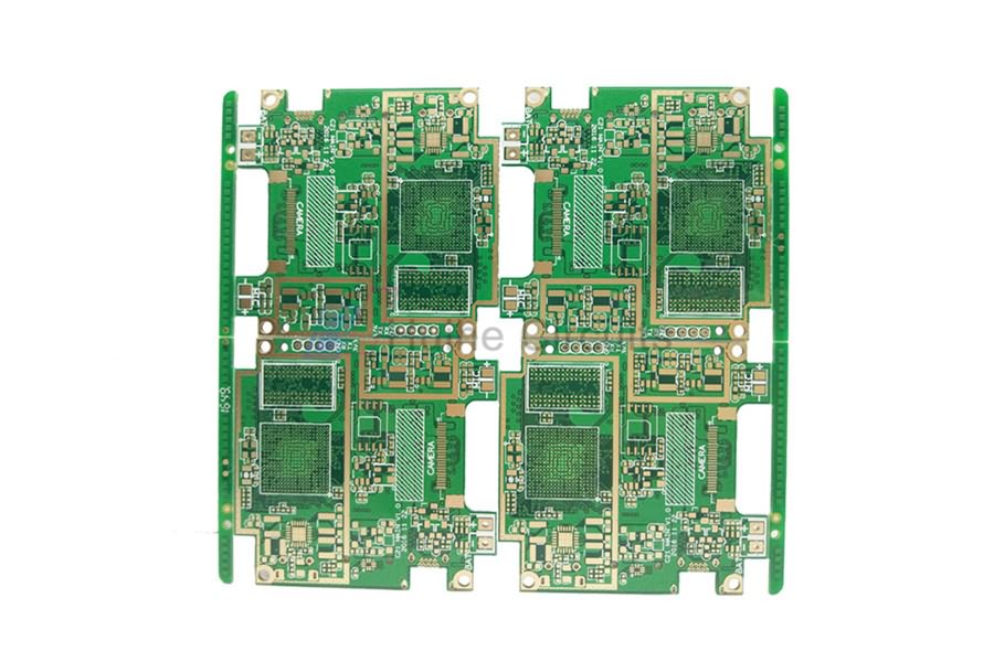
8 layers Of Double Via Level 1 HDI PCB
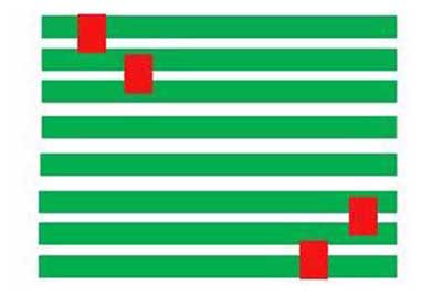
The figure below is 8 layers of level 2 cross blind vias , this processing methodand the above eight layers of second order stack hole , also need to play twolaser perforations . But the perforations are not stacked on top of each othermaking it much less difficult to process.
8 Layers Of Level 2 Cross Blind Vias PCB
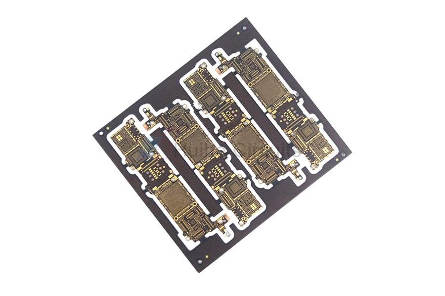
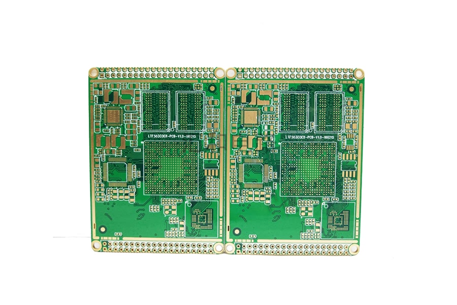
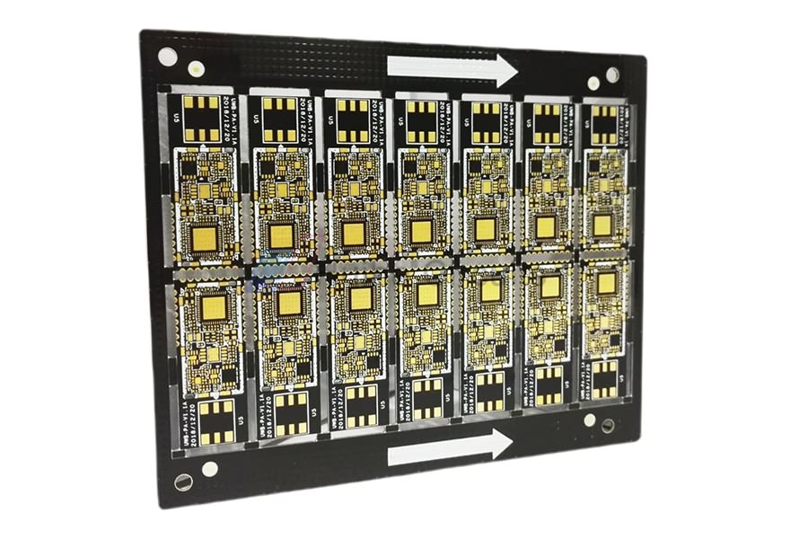
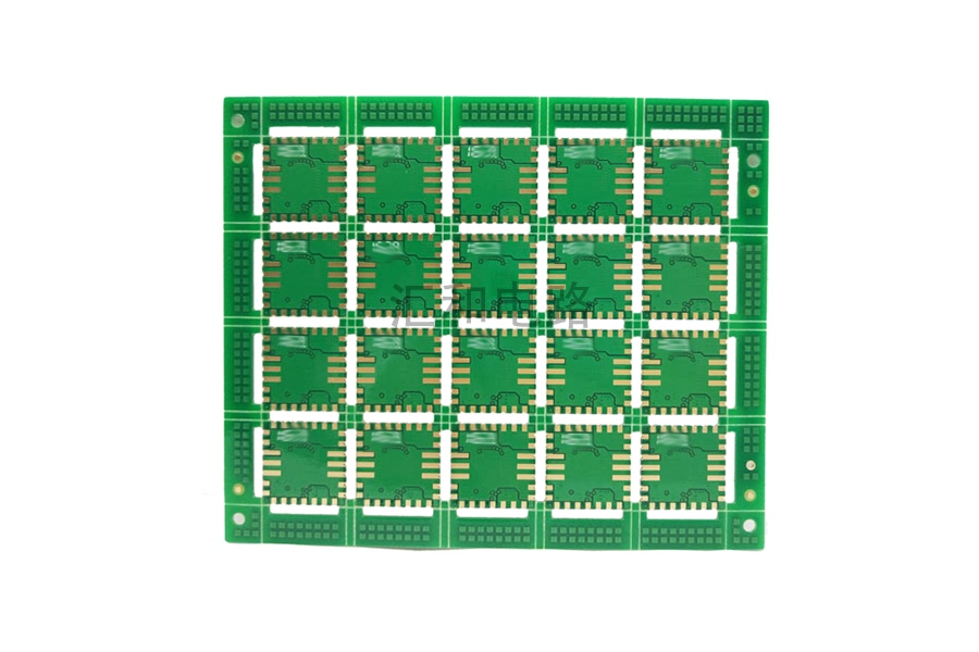
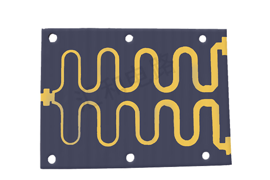
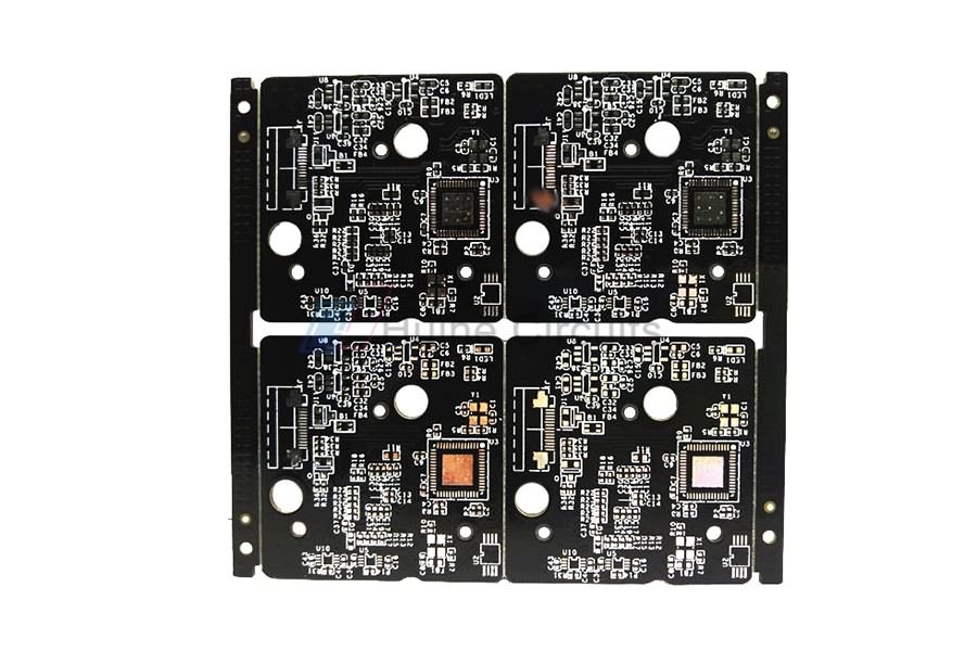
Product detail pictures:
Related Product Guide:
"Based on domestic market and expand abroad business" is our enhancement strategy for China Wholesale Wifi Pcb Board Manufacturers - 8 Layer ENIG Blind Buried Via PCB – Huihe , The product will supply to all over the world, such as: Bogota, Canberra, Liberia, We believe that good business relationships will lead to mutual benefits and improvement for both parties. We now have established long-term and successful cooperative relationships with many customers through their confidence in our customized services and integrity in doing business. We also enjoy a high reputation through our good performance. Better performance will be expected as our principle of integrity. Devotion and Steadiness will remain as ever.
This is a very professional wholesaler, we always come to their company for procurement, good quality and cheap.
-
China Wholesale Purple Pcbs Factories - 6 Laye...
-
China Wholesale Screen Printing Circuit Boards ...
-
China Wholesale Circuit Board Makers Pricelist ...
-
High Quality for Multilayer Pcb Prototype - 8 ...
-
China Wholesale Circuit Board Assembly Supplier...
-
China Wholesale Flex Printed Circuit Suppliers ...


