
China Wholesale Purple Pcbs Factories - 6 Layer ENIG impedance half hole PCB – Huihe
China Wholesale Purple Pcbs Factories - 6 Layer ENIG impedance half hole PCB – Huihe Detail:
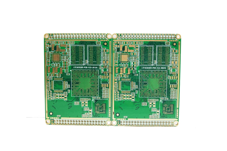
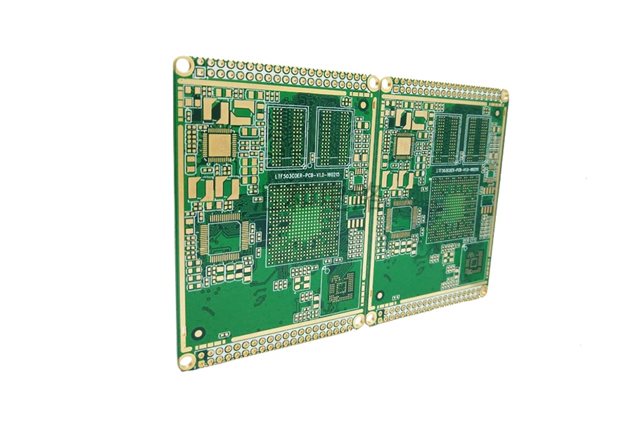
About Metallized Half Hole PCB
The metallized half hole is a half hole at the edge of the plate and is electroplated. Metallized semi-holes are mainly used for the direct connection between plates. They are mainly used to weld together two printed circuit boards with circuit design technology. The whole system takes up much less space than a PCB system using a row pin connector.
Design parameters of half hole PCB
|
Min. Hole Diameter |
Minimum pad |
Minimum pad spacing |
The distance between window and green |
Minimum size of solder bridge |
Minimum pin pitch |
|
500µm |
900µm |
250µm |
50µm-75µm |
100µm |
1150µm |
How are metallized half hole PCB made?
First, electroplated through holes are made on the edge of PCs or set (smaller unit in production board PNL), and then half of electroplated through-hole Gong is removed by using gong machine (milling machine), and the remaining half is half hole. Since copper is difficult to process and is likely to cause bit breakage, special gongs are required and higher speed is set to make the surface of hole wall and edge smoother.
Each half hole is then inspected by the semi-finished product inspection station. The minimum diameter of the half holes that can be manufactured by the confluence circuit is 0.5 mm, and the half holes should be at least 0.5 mm apart.
If you need to make a smaller half hole diameter, please contact our customer service personnel to communicate the feasibility plan. When placing a purchase order for a half hole plate to Huihe circuit, please communicate the details of the half hole plate with the technical engineer of Huihe circuit to ensure that you can obtain a cost-effective manufacturing solution.
How to identify a half hole in your design file ?
Half hole is designed because of the structure of the device and circuit board plug-in A single or whole rowof device holes are directly added to the outline of the metalized half hole to ensure that half of the deviceholes are in the board and half are out of the board . The Gerber file should contain the following:
01
Line layer(GTL and GBL)
Half hole brazing pads are located at top and bottom
02
Weld barer layer(GTS and GBS)
Weld barnier opening at half hole position
03
Hole layer (TXT/DRL)
The hole location of each half hole
04
Mechanical/profile layer(GMU/GKO)
The profile should be centered through each half hole
Our advantage
1. Own factory, factory area 12000 square meters, factory direct sales
2.20+ core technical personnel with more than 10 years of experience, proficient in industry standards and process quality.
3.Advanced equipment: automatic copper deposition / electroplating line, LDI / CCD exposure machine and other equipment to produce high quality and high reliability products
Application

Industrial control
Consumer electronics

Communication
Equipment display

Automatic Plating Line

PTH line

LDI

CCD Exposure Machine
Our factory


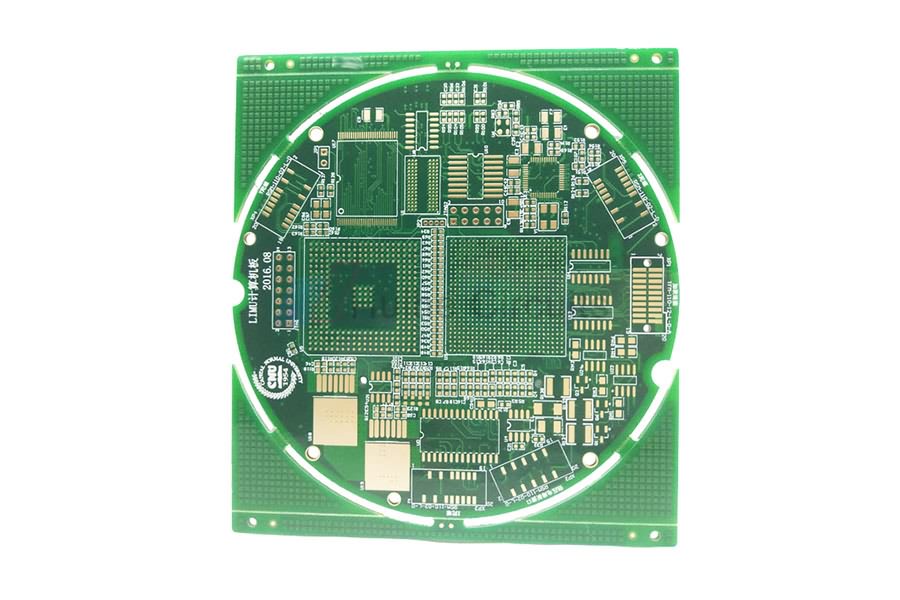
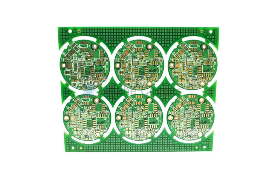
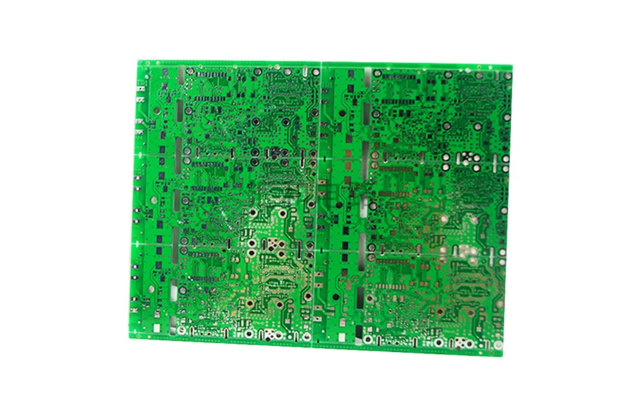
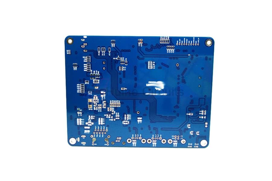
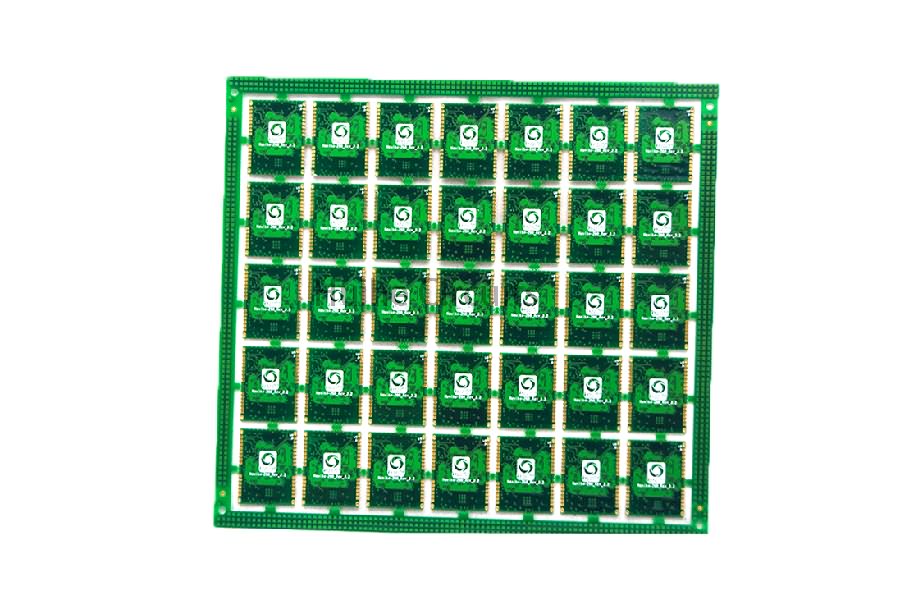
Product detail pictures:

Related Product Guide:
We take pleasure in an extremely fantastic standing among the our prospects for our great product top quality, competitive cost and the finest support for China Wholesale Purple Pcbs Factories - 6 Layer ENIG impedance half hole PCB – Huihe , The product will supply to all over the world, such as: Jamaica, Uzbekistan, Germany, Hard work to keep making progress, innovation in the industry, make every effort to first-class enterprise. We try our best to build the scientific management model, to learn abundant experienced knowledge, to develop advanced production equipment and production process , to create the first-call quality goods, reasonable price , high quality of service , quick delivery , to present you create new value .
A nice supplier in this industry, after a detail and careful discussion, we reached a consensus agreement. Hope that we cooperate smoothly.
-

China Wholesale Speaker Pcb Board Factories - ...
-
China Wholesale Rf Circuit Board Quotes - 12 L...
-
China Wholesale Embedded Pcb Manufacturers - 8...
-
China Wholesale Pcb Circuit Manufacturers - 2 ...
-
China Wholesale Main Printed Circuit Board Pric...
-
China Wholesale Rigid Flex Printed Circuit Boar...


