
China Wholesale Main Printed Circuit Board Pricelist - 6 Layer HASL Blind Buried Via PCB 13699 – Huihe
China Wholesale Main Printed Circuit Board Pricelist - 6 Layer HASL Blind Buried Via PCB 13699 – Huihe Detail:
Features of the Buried Via
The manufacturing process cannot be achieved by drilling after bonding. Drilling must be performed at individual circuit layers. The inner layer must be partially bonded first, followed by electroplating treatment, and then all bonded finally. This process is usually used only on high-density PCBs to increase the available space for other circuit layers
The basic process of making HDI blind buried Via PCB
Equipment display

Automatic Plating Line

PTH line

LDI

CCD Exposure Machine
Application

Communications

Security electronics

Railtransit
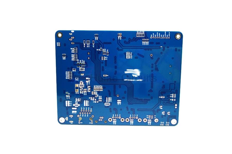
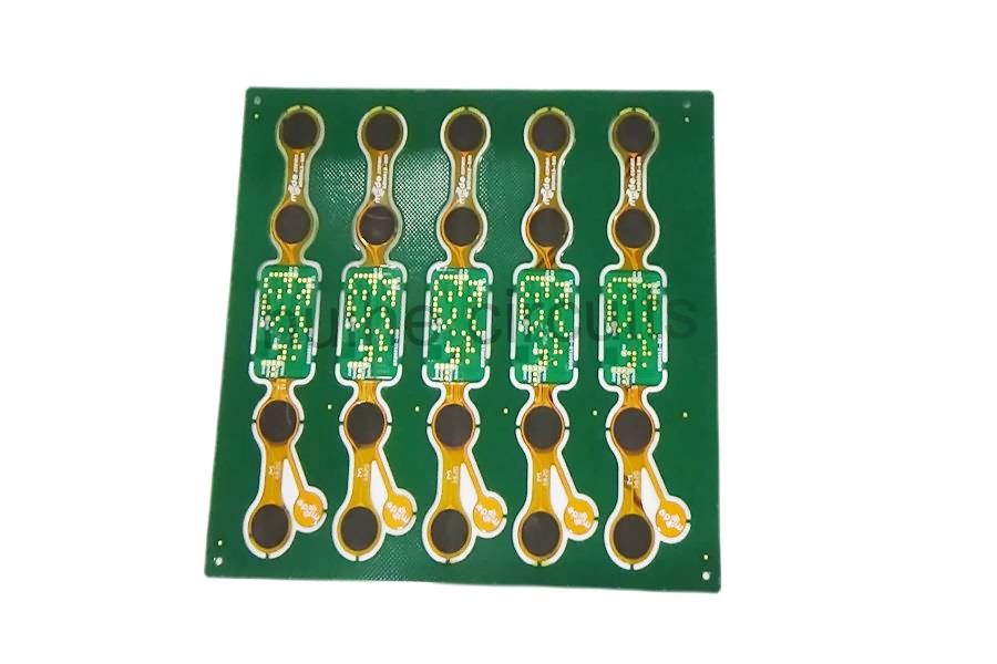
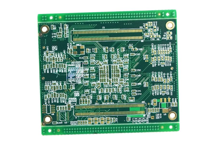
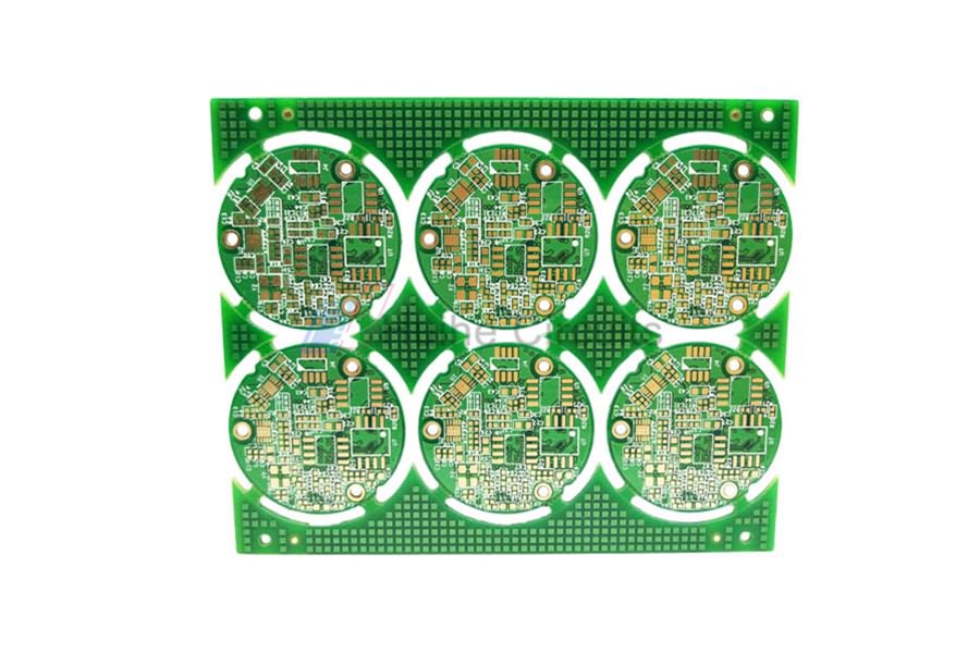
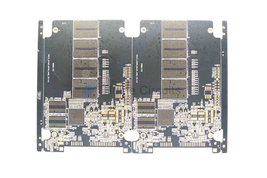
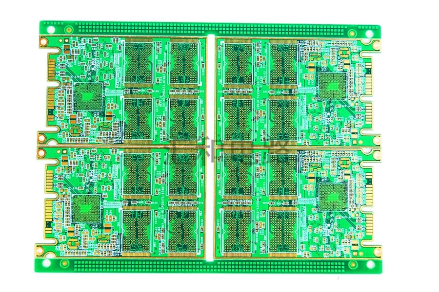
Product detail pictures:


Related Product Guide:
Our well-equipped facilities and superb good quality control throughout all stages of manufacturing enables us to guarantee total buyer gratification for China Wholesale Main Printed Circuit Board Pricelist - 6 Layer HASL Blind Buried Via PCB 13699 – Huihe , The product will supply to all over the world, such as: Anguilla, Paris, Somalia, During in 11 years, We have participated in more than 20 exhibitions, obtains the highest praise from each customer. Our company has been devoting that "customer first" and committed to helping customers expand their business, so that they become the Big Boss !
It's really lucky to find such a professional and responsible manufacturer, the product quality is good and delivery is timely, very nice.
Write your message here and send it to us
-
China Wholesale Stabilizer Circuit Board Pricel...
-
China Wholesale Rigid Printed Circuit Board Fac...
-
China Wholesale Motherboard Circuit Board Quote...
-
China Wholesale Main Pcb Quotes - 6 Layer ENIG...
-
China Wholesale Fast Pcb Prototyping Manufactur...
-

China Wholesale Flexible Circuit Board Quotes -...


