
Super Purchasing for 4 Layer Pcb Cost - 6 Layer HASL Blind Buried Via PCB – Huihe
Super Purchasing for 4 Layer Pcb Cost - 6 Layer HASL Blind Buried Via PCB – Huihe Detail:
Features Of The Buried Via PCB
The manufacturing process cannot be achieved by drilling after bonding. Drilling must be performed at individual circuit layers. The inner layer must be partially bonded first, followed by electroplating treatment, and then all bonded finally. This process is usually used only on high-density PCBs to increase the available space for other circuit layers
The Basic Process Of HDI Blind Buried Via PCB
Equipment Display

PCB Automatic Plating Line

PCB PTH Line

PCB LDI

PCB CCD Exposure Machine
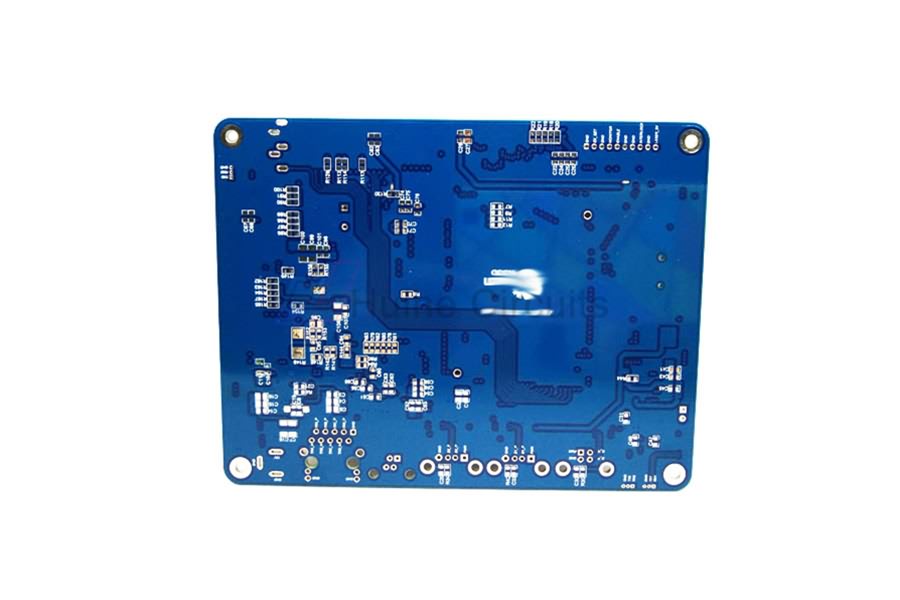
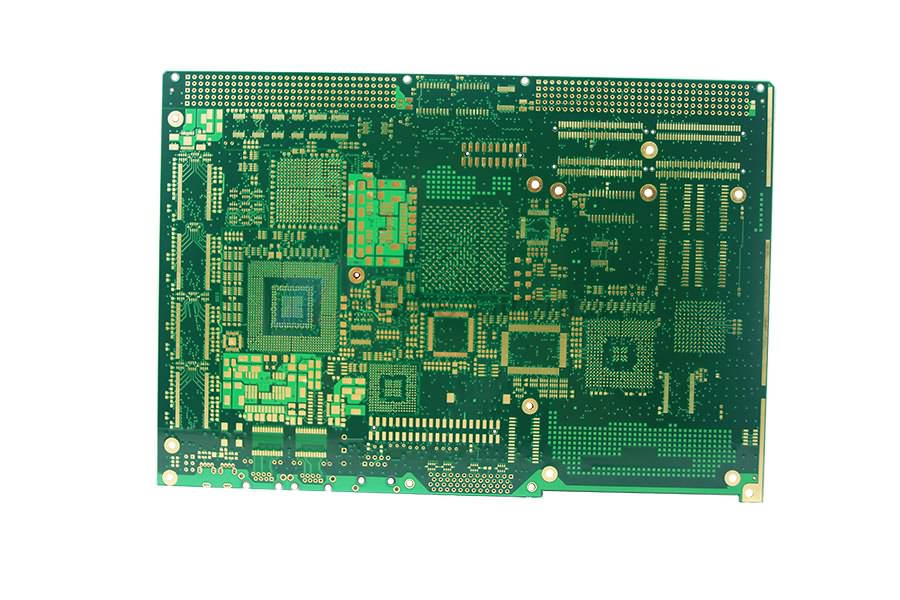
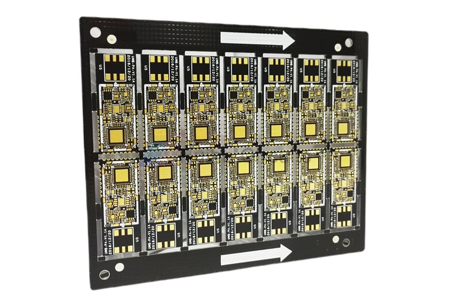
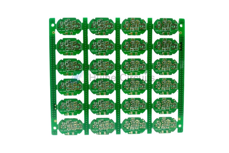
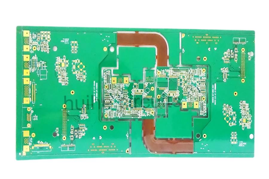
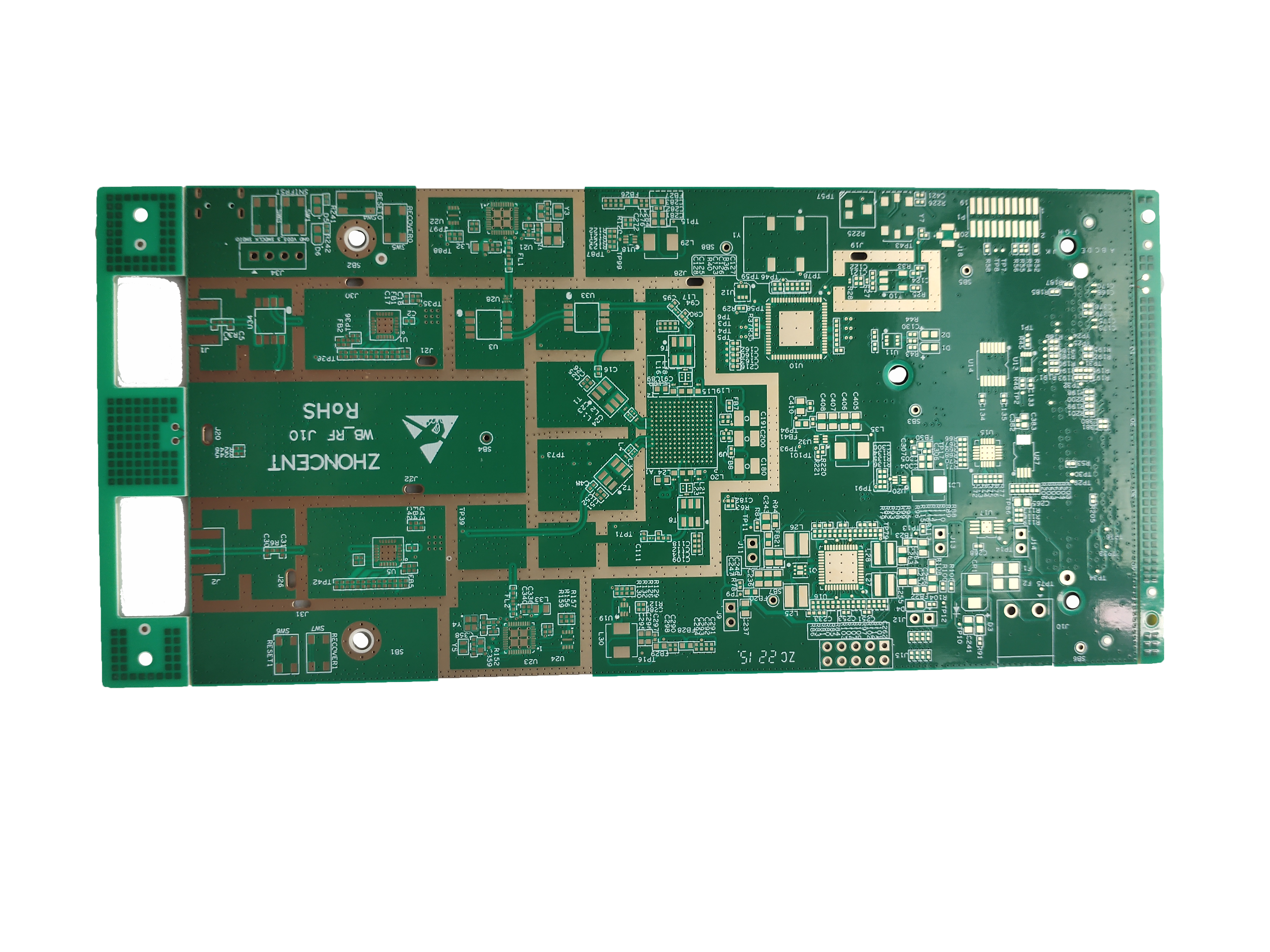
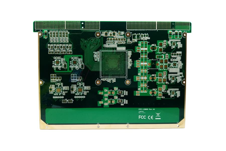
Product detail pictures:


Related Product Guide:
To create much more price for clients is our company philosophy; purchaser growing is our working chase for Super Purchasing for 4 Layer Pcb Cost - 6 Layer HASL Blind Buried Via PCB – Huihe , The product will supply to all over the world, such as: Luxembourg, panama, Libya, Abiding by our motto of "Hold well the quality and services, Customers Satisfaction", So we give our clients with high quality products and solutions and excellent service. Be sure to feel free to contact us for further information.
This company can be well to meet our needs on product quantity and delivery time, so we always choose them when we have procurement requirements.
Write your message here and send it to us
-
18 Years Factory High Frequency Pcb Manufacture...
-
China Wholesale Rohs Pcb Pricelist - 6 Layer E...
-
China Wholesale Tht Pcb Suppliers - 6 Layer EN...
-
Factory Outlets China Fpc - 8 Layer FPC+FR4 Ri...
-
Reasonable price 0.4 Mm Pcb - 12 Layer ENIG FR...
-
Hot New Products Rigid Printed Circuit Board Qu...


