
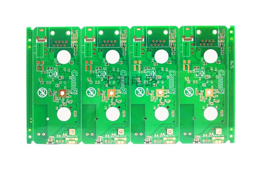
professional factory for Pcb Tg150 - 8 Layer ENIG FR4 Buried Vias PCB – Huihe
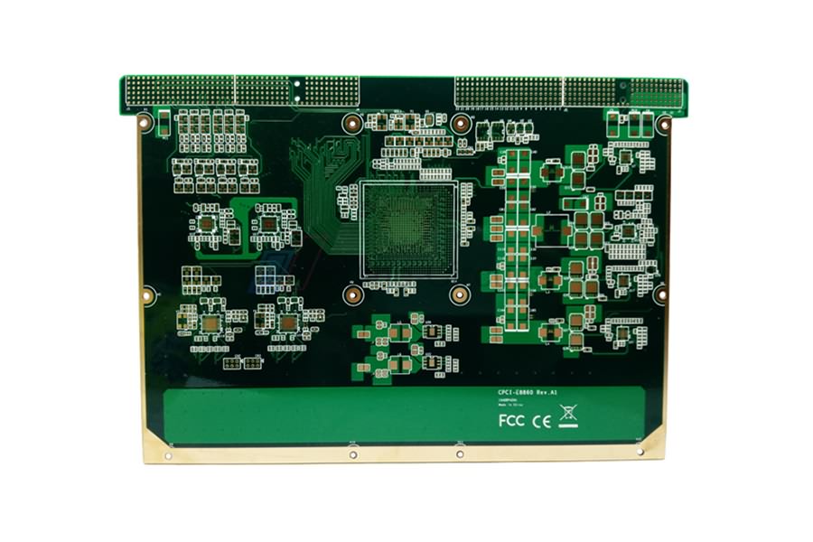
professional factory for Pcb Tg150 - 8 Layer ENIG FR4 Buried Vias PCB – Huihe Detail:
Deficiencies Of the Blind Buried Vias PCB
The main problem of blind buried via PCB is the high cost. In contrast, buried holes cost less than blind holes, but the use of both types of holes can significantly increase the cost of a board. The cost increase is due to the more complex manufacturing process of the blind buried hole, that is, the increase in manufacturing processes also leads to the increase in testing and inspection processes.
Buried Via PCB
Buried via PCBs are used to connect different inner layers, but have no connection with the outermost layer.A separate drill file must be generated for each level of buried hole. The ratio of hole depth to aperture (aspect ratio/thickness-diameter ratio) must be less than or equal to 12.
The keyhole determines the depth of the keyhole, the maximum distance between different inner layers.In general, the larger the inner hole ring, the more stable and reliable the connection.
Blind Buried Vias PCB
The main problem of blind buried via PCB is the high cost. In contrast, buried holes cost less than blind holes, but the use of both types of holes can significantly increase the cost of a board. The cost increase is due to the more complex manufacturing process of the blind buried hole, that is, the increase in manufacturing processes also leads to the increase in testing and inspection processes.
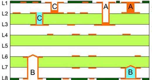
A: buried vias
B: Laminated buried via (not recommended)
C: Cross buried via
The advantage of blind Vias and buried Vias for engineers is the increase of component density without increasing layer number and size of circuit board. For electronic products with narrow space and small design tolerance, blind hole design is a good choice. The use of such holes helps the circuit design engineer to design a reasonable hole/pad ratio to avoid excessive ratios.
Factory Show

PCB Manufacturing Base

Admin Receptionist

Meeting Room

General Office
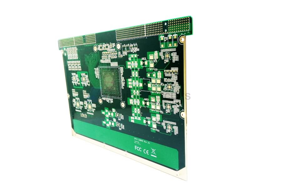
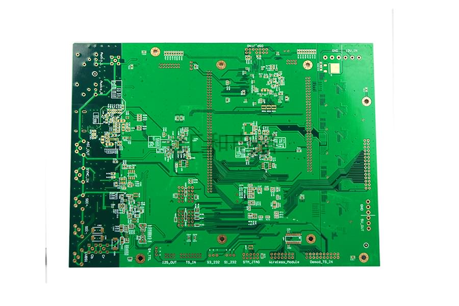
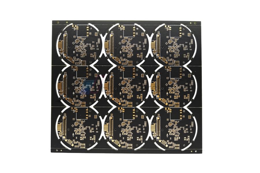
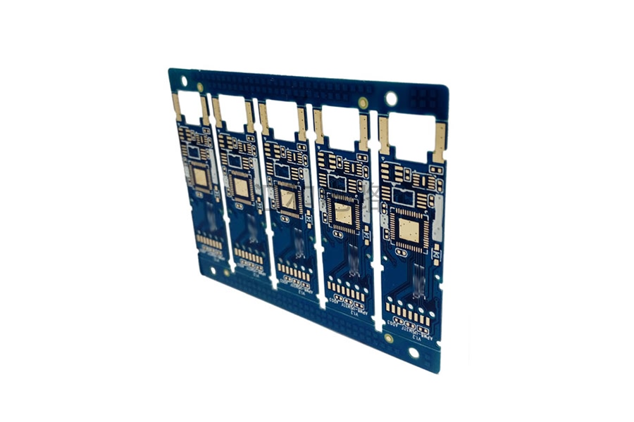
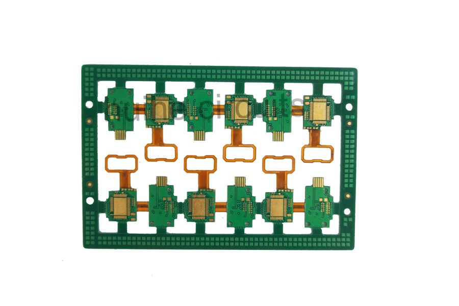
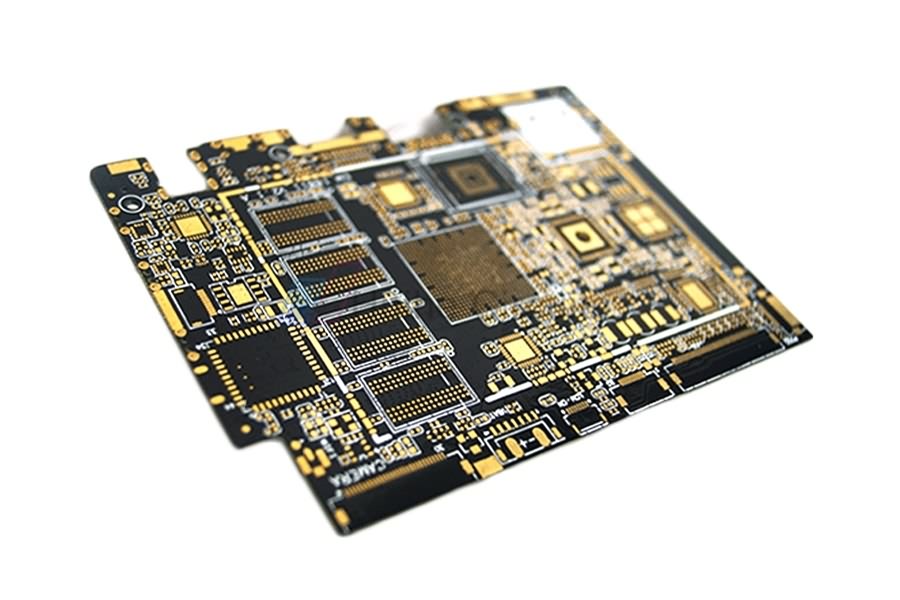
Product detail pictures:

Related Product Guide:
With a positive and progressive attitude to customer's curiosity, our organization repeatedly improves our products top quality to meet the wants of consumers and further focuses on safety, reliability, environmental necessities, and innovation of professional factory for Pcb Tg150 - 8 Layer ENIG FR4 Buried Vias PCB – Huihe , The product will supply to all over the world, such as: Southampton, Barcelona, Peru, On today, we've got customers from all over the world, including USA, Russia, Spain, Italy, Singapore, Malaysia, Thailand, Poland, Iran and Iraq. The mission of our company is to deliver the highest quality products with best price. We've been looking forward to doing business with you!
The company's products very well, we have purchased and cooperated many times, fair price and assured quality, in short, this is a trustworthy company!
-
China Wholesale Printed Circuit Board Component...
-
Factory Supply Multilayer Board Manufacturers -...
-
China Wholesale Pwb Printed Wiring Board Pricel...
-
China Wholesale Pcb Service Pricelist - 4 Laye...
-
China Wholesale Fast Pcb Prototyping Factories ...
-
China Wholesale Smt Circuit Boards Manufacturer...


