
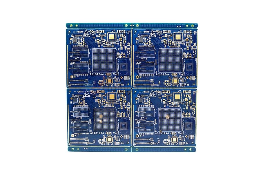
OEM China Pcb Fabrication Prototype - 4 Layer ENIG FR4 Half Hole PCB – Huihe
OEM China Pcb Fabrication Prototype - 4 Layer ENIG FR4 Half Hole PCB – Huihe Detail:
Conventional Metallized Half-Hole PCB Fabrication Process
Drilling — Chemical Copper — Full Plate Copper — Image Transfer — Graphics Electroplating — Defilm — Etching — Stretch Soldering — Half Hole Surface Coating (Shaped at the Same Time with the Profile).
The metallized half hole is cut in half after the round hole is formed. It is easy to appear the phenomenon of copper wire residue and copper leather warping in the half hole, which affects the function of the half hole and leads to the decrease of product performance and yield. In order to overcome the above defects, it shall be carried out according to the following process steps of metallized semi-orifice PCB:
1. Processing half hole double V type knife.
2. In the second drill, the guide hole is added on the edge of the hole, the copper skin is removed in advance, and the burr is reduced. The grooves are used for drilling to optimize the speed of falling.
3. Copper plating on the substrate, so that a layer of copper plating on the hole wall of the round hole on the edge of the plate.
4. The outer circuit is made by compression film, exposure and development of the substrate in turn, and then the substrate is plated with copper and tin twice, so that the copper layer on the hole wall of the round hole on the edge of the plate is thickened and the copper layer is covered by the tin layer with anti-corrosion effect;
5. Half hole forming plate edge round hole cut in half to form a half hole;
6. Removing the film will remove the anti-plating film pressed in the process of film pressing;
7. Etch the substrate, and remove the exposed copper etching on the outer layer of the substrate after removing the film;Tin peeling The substrate is peeled so that the tin is removed from the semi-perforated wall and the copper layer on the semi-perforated wall is exposed.
8. After molding, use red tape to stick the unit plates together, and over alkaline etching line to remove burrs
9. After secondary copper plating and tin plating on the substrate, the circular hole on the edge of the plate is cut in half to form a half hole. Because the copper layer of the hole wall is covered with tin layer, and the copper layer of the hole wall is completely connected with the copper layer of the outer layer of the substrate, and the binding force is large, the copper layer on the hole wall can be effectively avoided when cutting, such as pulling off or the phenomenon of copper warping;
10. After the completion of the semi-hole forming and then remove the film, and then etch, copper surface oxidation will not occur, effectively avoid the occurrence of copper residue and even short circuit phenomenon, improve the yield of metallized semi-hole PCB.
Equipment Display

PCB Automatic Plating Line

PCB PTH Line

PCB LDI

PCB CCD Exposure Machine
Factory Show

PCB Manufacturing Base

Admin Receptionist

Meeting Room

General Office
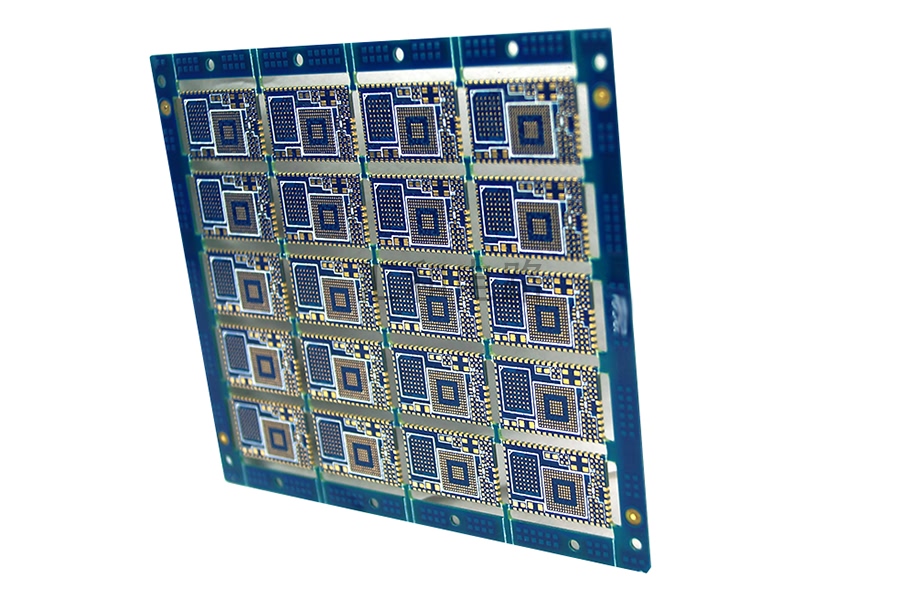
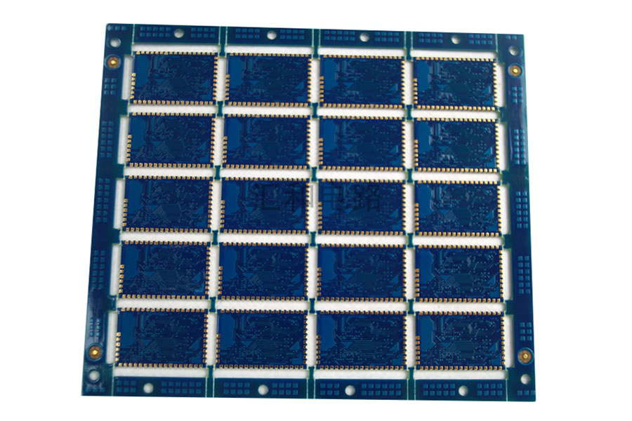
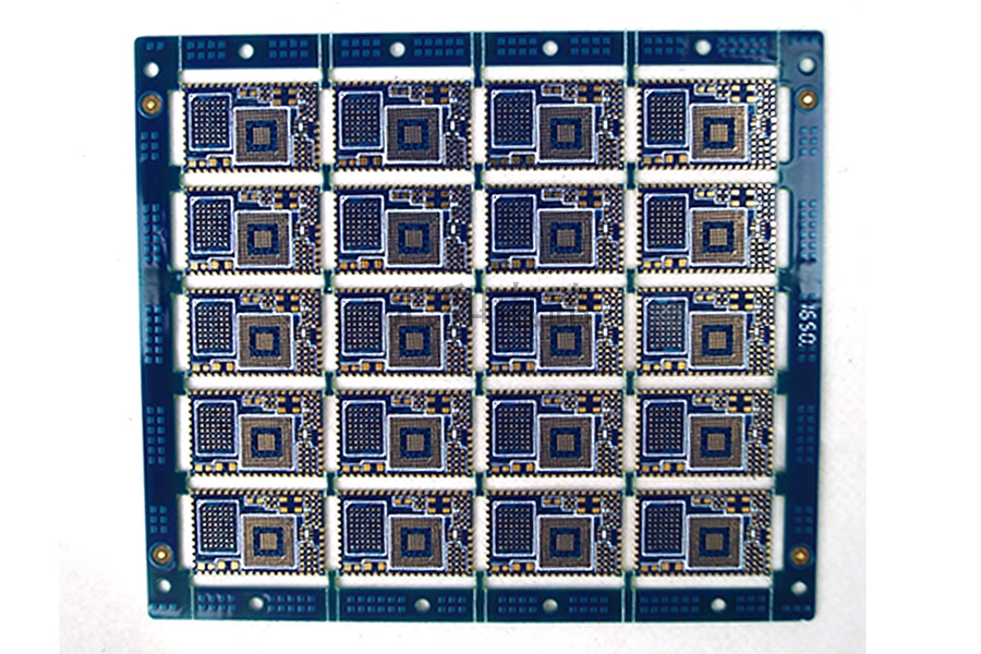
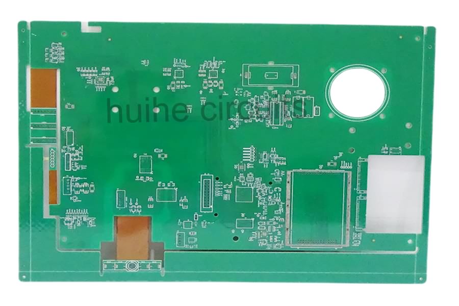
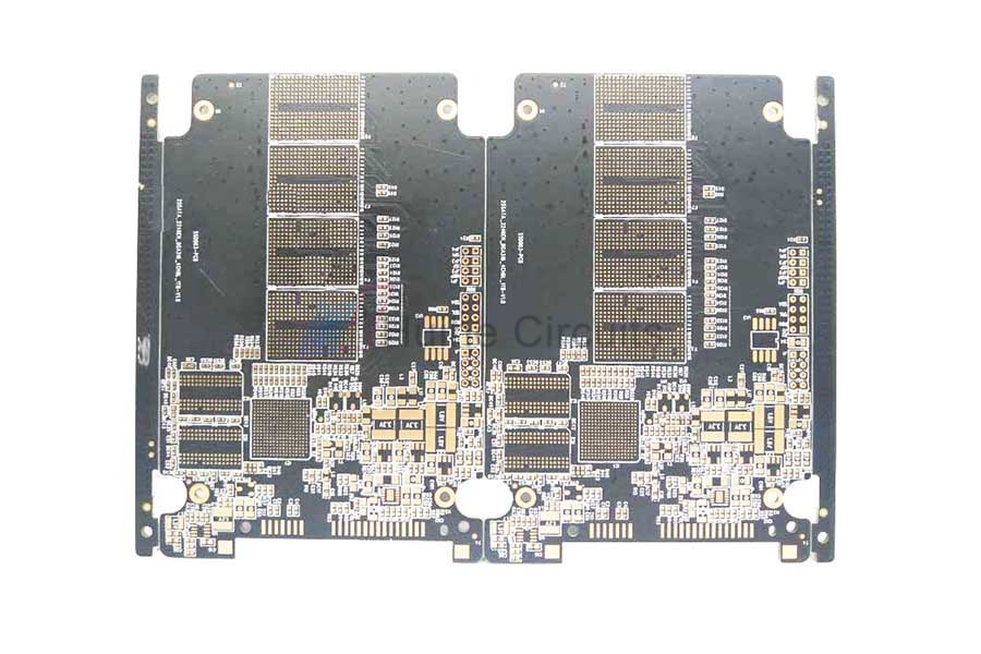
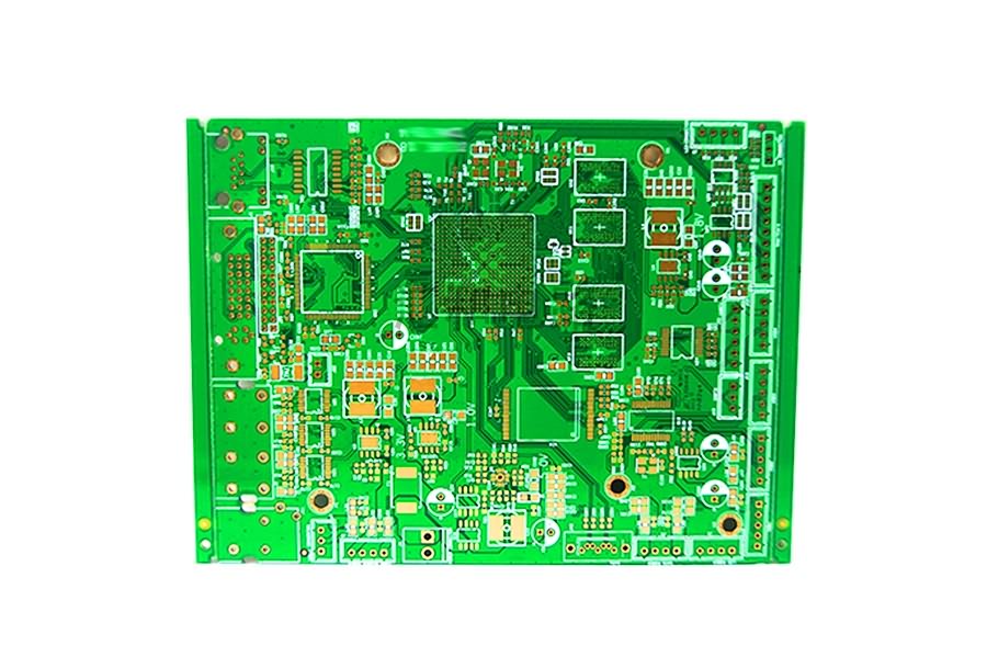
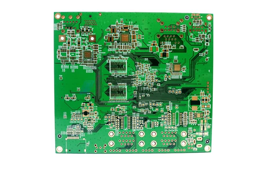
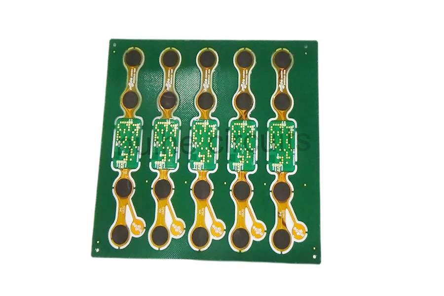
Product detail pictures:

Related Product Guide:
Our solutions are widely regarded and trustworthy by consumers and may meet continually modifying financial and social requirements for OEM China Pcb Fabrication Prototype - 4 Layer ENIG FR4 Half Hole PCB – Huihe , The product will supply to all over the world, such as: Kuwait, Canada, venezuela, Thus far, our item associated with printer dtg a4 may be shown in most foreign nations as well as urban centers, which are sought after simply by targeted traffic. We all highly imagine that now we have the full capacity to present you with contented merchandise. Desire to collect requests of your stuff and produce the long-term co-operation partnership. We very seriously promise:Csame top quality, better price; exact same selling price, higher quality.
The company has a good reputation in this industry, and finally it tured out that choose them is a good choice.
-
China Wholesale Wifi Pcb Board Quotes - 8 Laye...
-
China Wholesale Multilayer Pcb Board Pricelist ...
-
China Gold Supplier for Fpc Flexible Pcb In She...
-
China Wholesale Incubator Circuit Board Quotes ...
-
Trending Products Hal Pcb - 4 Layer ENIG FPC+F...
-
China Wholesale Main Pcb Board Manufacturers -...


