
Manufacturer of 14 Layer Circuit Board Manufacturer - 10 Layer ENIG FR4 Via In Pad PCB – Huihe
Manufacturer of 14 Layer Circuit Board Manufacturer - 10 Layer ENIG FR4 Via In Pad PCB – Huihe Detail:
Via In Pad PCB
In PCB design, a through-hole is a spacer with a small plated hole in the printed circuit board to connect the copper rails on each layer of the board. There is a type of through-hole called microhole, which only has a visible blind hole in one surface of a high-density multilayer PCB or an invisible buried hole in either surface. The introduction and wide application of high-density pin parts, as well as the need for small size PCBS, have brought new challenges. Therefore, a better solution to this challenge is to use the latest but popular PCB manufacturing technology called “Via in Pad”.
In current PCB designs, rapid use of via in pad is required due to the decreasing spacing of part footprints and the miniaturization of PCB shape coefficients. More importantly, it enables signal routing in as few areas of the PCB layout as possible and, in most cases, even avoids bypassing the perimeter occupied by the device.
Pass-through pads are very useful in high speed designs as they reduce track length and hence inductance. You’d better check to see if your PCB manufacturer has enough equipment to make your board, as this may cost more money. However, if you cannot place through the gasket, place directly and use more than one to reduce inductance.
In addition, the pass pad can also be used in the case of insufficient space, such as in the micro-BGA design, which cannot use the traditional fan-out method. There is no doubt that the defects of the through hole in the welding disc are small, because of the application in the welding disc, the impact on the cost is great. The complexity of manufacturing process and the price of basic materials are two main factors that affect the production cost of conductive filler. First, Via in Pad is an additional step in the PCB manufacturing process. However, as the number of layers decreases, so do the additional costs associated with Via in Pad technology.
Advantages Of Via In Pad PCB
Via in pad PCBs have many advantages. First, it facilitates increased density, the use of finer spacing packages, and reduced inductance. What’s more, in the process of via in pad, a via is directly placed below the contact pads of the device, which can achieve greater part density and superior routing. So it can save a great quantity PCB spaces with via in pad for PCB designer.
Compared with blind vias and buried vias, via in pad has the following advantages:
Suitable for detail distance BGA;
Improve PCB density, save space;
Increase heat dissipation;
A flat and coplanar with component accessories is provided;
Because there is no trace of dog bone pad, inductance is lower;
Increase the voltage capacity of the channel port;
Via In Pad Application For SMD
1. Plug the hole with resin and plate it with copper
Compatible with small BGA VIA in Pad; First, the process involves filling holes with conductive or non-conductive material, and then plating the holes on the surface to provide a smooth surface for the weldable surface.
A pass hole is used in a pad design to mount components on the pass hole or to extend solder joints to the pass hole connection.
2. The microholes and holes are plated on the pad
Microholes are IPC based holes with a diameter of less than 0.15mm. It can be a through hole (related to aspect ratio), however, usually the microhole is treated as a blind hole between two layers; Most of the microholes are drilled with lasers, but some PCB manufacturers are also drilling with mechanical bits, which are slower but cut beautifully and cleanly; The Microvia Cooper Fill process is an electrochemical deposition process for multilayer PCB manufacturing processes, also known as Capped VIas; Although the process is complex, it can be made into HDI PCBS that most PCB manufacturers will get filled with microporous copper.
3. Block the hole with welding resistance layer
It is free and compatible with large solder SMD pads; The standardized LPI resistance welding process cannot form a filled through hole without the risk of bare copper in the hole barrel. Generally, it can be used after a second screen printing by depositing UV or heat-cured epoxy solder resistances into the holes to plug them; It is called through blockage. Through-hole plugging is the blocking of through-holes with an resist material to prevent air leakage when testing the plate, or to prevent short circuits of elements near the surface of the plate.
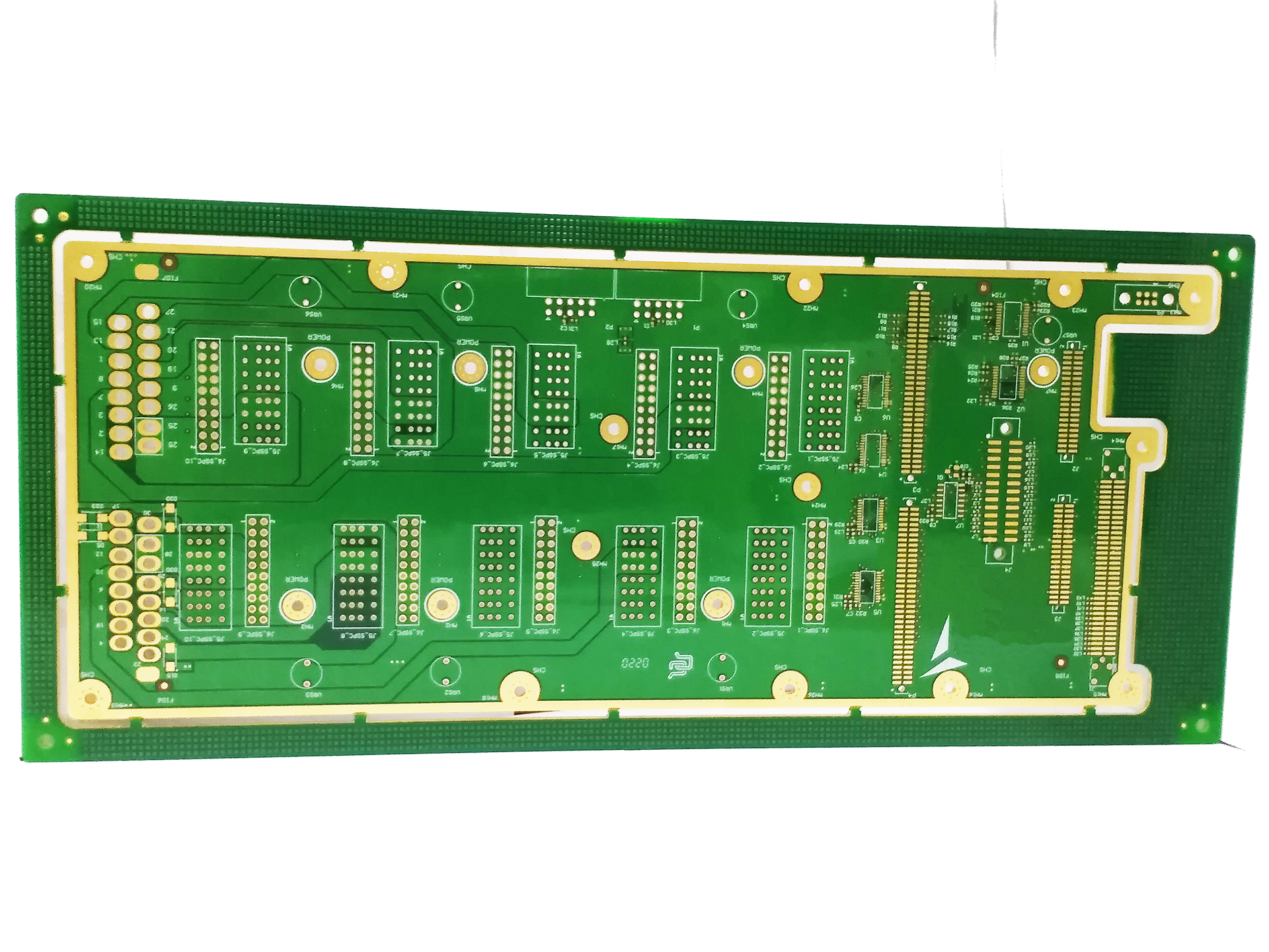
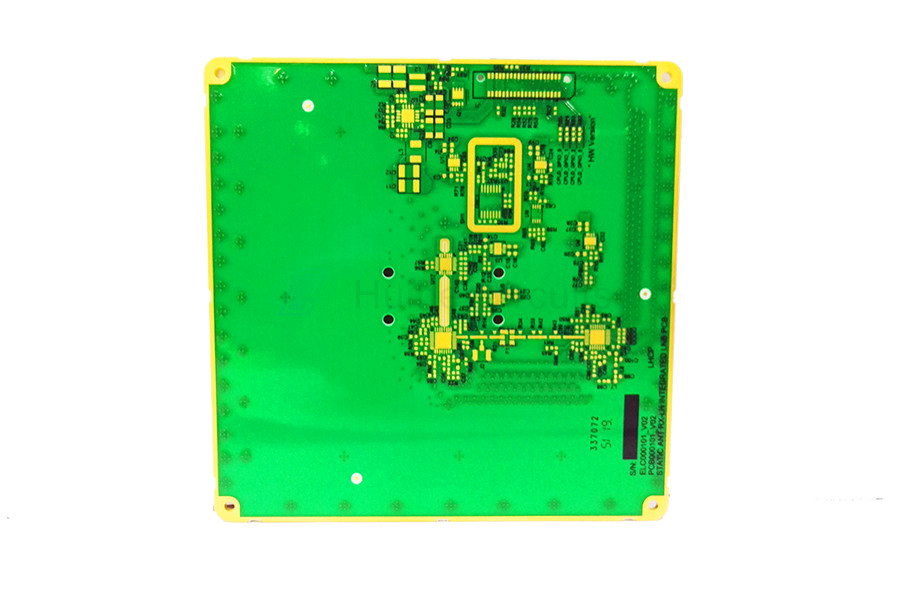
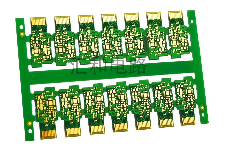
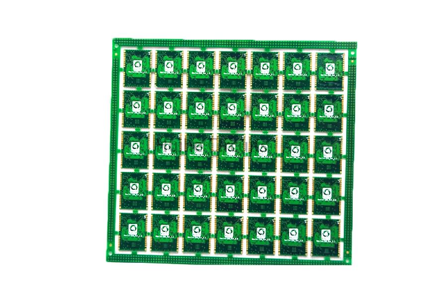
Product detail pictures:
.png)
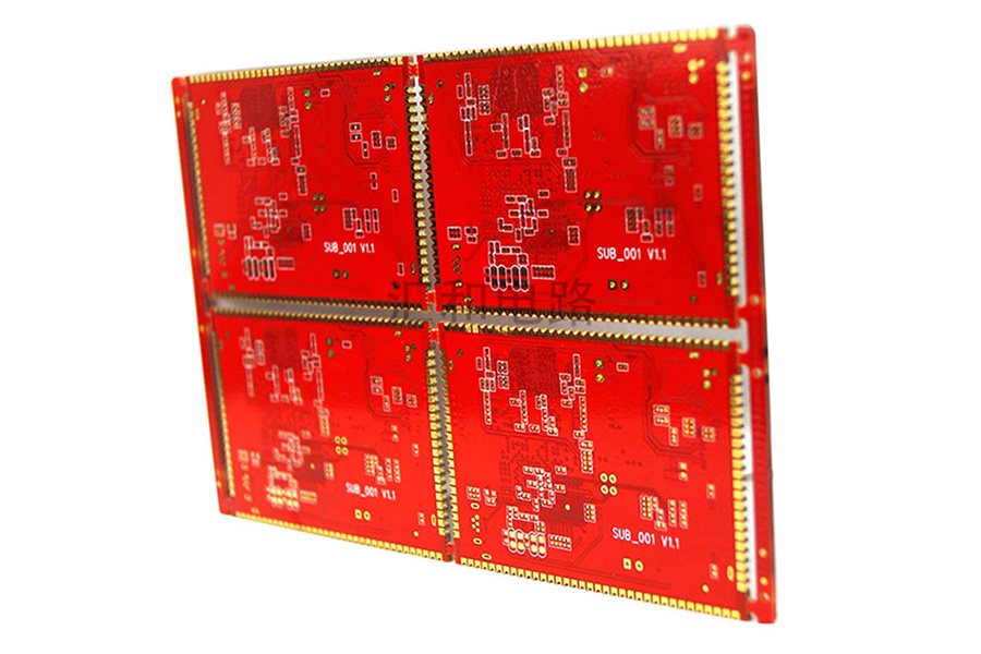
Related Product Guide:
We support our prospective buyers with ideal top quality merchandise and superior level provider. Becoming the specialist manufacturer in this sector, we have now attained abundant practical expertise in producing and managing for Manufacturer of 14 Layer Circuit Board Manufacturer - 10 Layer ENIG FR4 Via In Pad PCB – Huihe , The product will supply to all over the world, such as: Uruguay, Venezuela, Brisbane, Selling our products and solutions causes no risks and brings high returns to your company instead. It is our consistent pursuit to create value for clients. Our company is looking for agents sincerely. What are you waiting for? Come and join us. Now or never.
We have been engaged in this industry for many years, we appreciate the work attitude and production capacity of the company, this is a reputable and professional manufacturer.
-
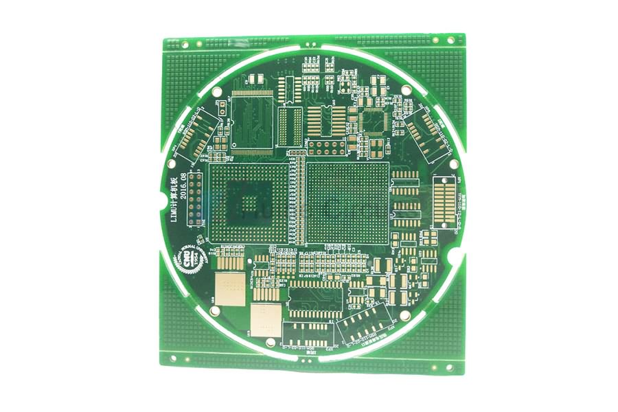
China Wholesale Round Pcb Suppliers - 8 Layer ...
-
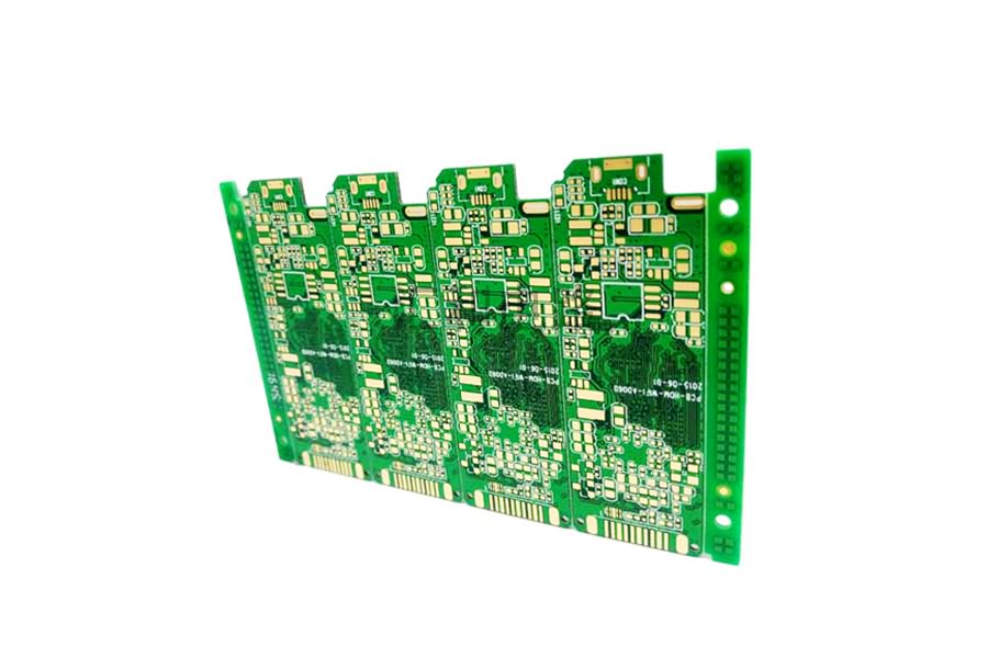
China Wholesale Printed Circuit Board Component...
-
China Wholesale Populated Printed Circuit Board...
-
China Wholesale Order Printed Circuit Board Quo...
-
China Wholesale Prototype Pcb Fabrication Manuf...
-
China Wholesale Stabilizer Circuit Board Manufa...


