Hot Selling for Quick Turn Pcb Manufacturer - 14 Layer ENIG FR4 Buried Via PCB – Huihe
Hot Selling for Quick Turn Pcb Manufacturer - 14 Layer ENIG FR4 Buried Via PCB – Huihe Detail:
About Blind Buried Via PCB
Blind vias and buried vias are two ways to establish connections between layers of printed circuit board. The blind vias of the printed circuit board are copper-plated vias that can be connected to the outer layer through most of the inner layer. The burrow connects two or more inner layers but does not penetrate the outer layer. Use microblind vias to increase line distribution density, improve radio frequency and electromagnetic interference, heat conduction, applied to servers, mobile phones, digital cameras.
Buried Vias PCB
The buried Vias connects two or more inner layers but does not penetrate the outer layer
|
Min Hole Diameter/mm |
Min ring/mm |
via-in-pad Diameter/mm |
Maximum Diameter/mm |
Aspect Ratio |
|
|
Blind Vias(conventional) |
0.1 |
0.1 |
0.3 |
0.4 |
1:10 |
|
Blind Vias(special product) |
0.075 |
0.075 |
0.225 |
0.4 |
1:12 |
Blind Vias PCB
Blind Vias is to connect an outer layer to at least one inner layer
|
|
Min. Hole Diameter/mm |
Minimum ring/mm |
via-in-pad Diameter/mm |
Maximum Diameter/mm |
Aspect Ratio |
|
Blind Vias(mechanical drilling) |
0.1 |
0.1 |
0.3 |
0.4 |
1:10 |
|
Blind Vias(Laser drilling) |
0.075 |
0.075 |
0.225 |
0.4 |
1:12 |
The advantage of blind Vias and buried Vias for engineers is the increase of component density without increasing layer number and size of circuit board. For electronic products with narrow space and small design tolerance, blind hole design is a good choice. The use of such holes helps the circuit design engineer to design a reasonable hole/pad ratio to avoid excessive ratios.
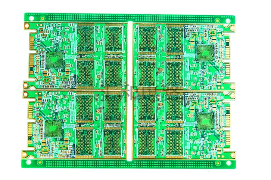
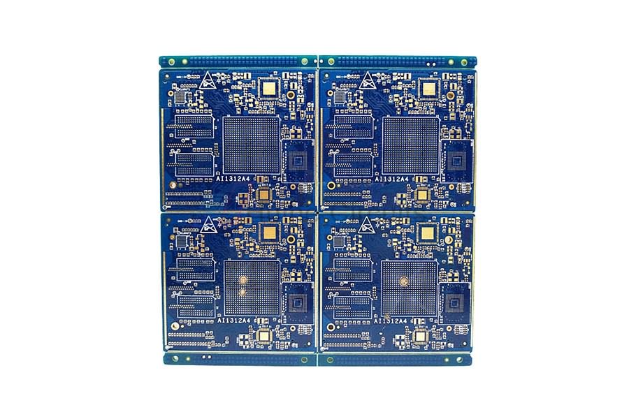
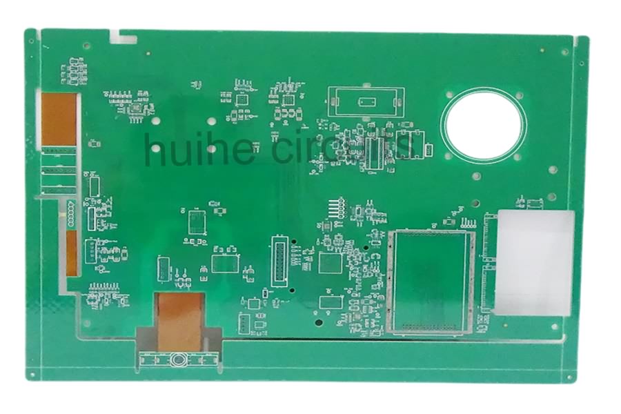
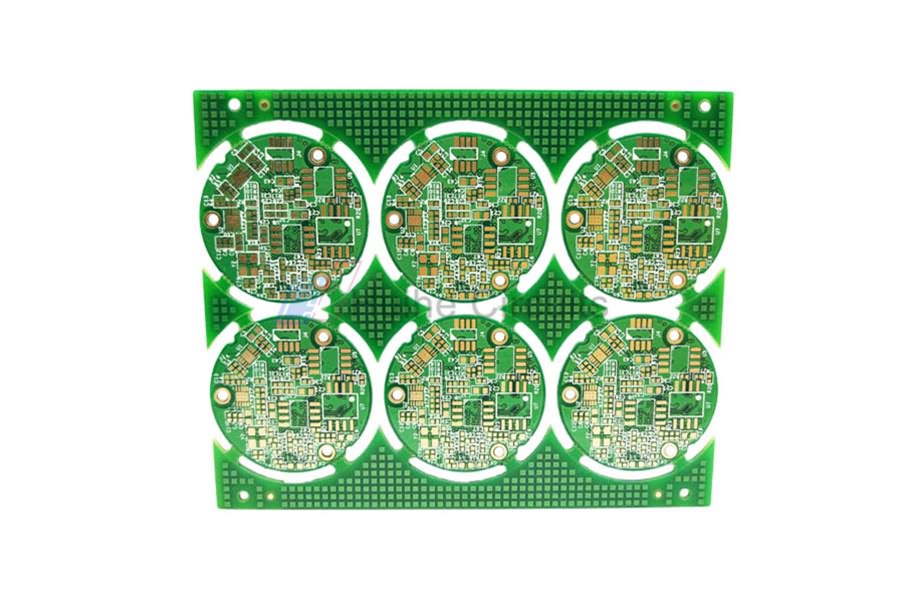
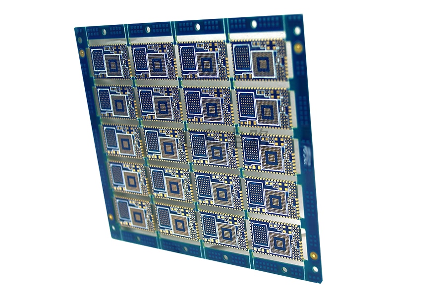
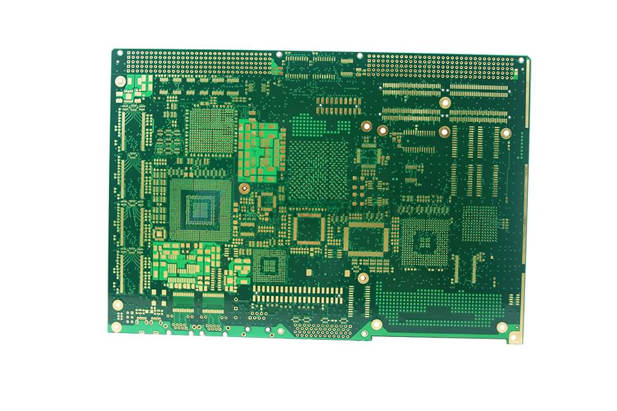
Product detail pictures:


Related Product Guide:
We have many excellent staff members good at marketing, QC, and dealing with kinds of troublesome problem in the production process for Hot Selling for Quick Turn Pcb Manufacturer - 14 Layer ENIG FR4 Buried Via PCB – Huihe , The product will supply to all over the world, such as: Bangladesh, Florida, Grenada, Why we can do these? Because: A, We are honest and reliable. Our products have high quality, attractive price, sufficient supply capacity and perfect service. B, Our geographical position has a big advantage . C, Various types: Welcome your inquiry, It will be highly appreciated.
In general, we are satisfied with all aspects, cheap, high-quality, fast delivery and good procuct style, we will have follow-up cooperation!